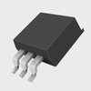
Part Details for FDB088N08 by Fairchild Semiconductor Corporation
Results Overview of FDB088N08 by Fairchild Semiconductor Corporation
- Distributor Offerings: (1 listing)
- Number of FFF Equivalents: (0 replacements)
- CAD Models: (Request Part)
- Number of Functional Equivalents: (0 options)
- Part Data Attributes: (Available)
- Reference Designs: (Not Available)
Tip: Data for a part may vary between manufacturers. You can filter for manufacturers on the top of the page next to the part image and part number.
FDB088N08 Information
FDB088N08 by Fairchild Semiconductor Corporation is a Power Field-Effect Transistor.
Power Field-Effect Transistors are under the broader part category of Transistors.
A transistor is a small semiconductor device used to amplify, control, or create electrical signals. When selecting a transistor, factors such as voltage, current rating, gain, and power dissipation must be considered, with common types. Read more about Transistors on our Transistors part category page.
Price & Stock for FDB088N08
| Part # | Distributor | Description | Stock | Price | Buy | |
|---|---|---|---|---|---|---|
|
|
Win Source Electronics | MOSFET N-CH 75V 75A D2PAK | 25290 |
|
$1.4432 / $2.1647 | Buy Now |
Part Details for FDB088N08
FDB088N08 CAD Models
FDB088N08 Part Data Attributes
|
|
FDB088N08
Fairchild Semiconductor Corporation
Buy Now
Datasheet
|
Compare Parts:
FDB088N08
Fairchild Semiconductor Corporation
Power Field-Effect Transistor, 85A I(D), 75V, 0.0088ohm, 1-Element, N-Channel, Silicon, Metal-oxide Semiconductor FET, TO-263AB, ROHS COMPLIANT, D2PAK-3
|
| Pbfree Code | Yes | |
| Rohs Code | Yes | |
| Part Life Cycle Code | Transferred | |
| Ihs Manufacturer | FAIRCHILD SEMICONDUCTOR CORP | |
| Part Package Code | D2PAK | |
| Package Description | ROHS COMPLIANT, D2PAK-3 | |
| Pin Count | 2 | |
| Manufacturer Package Code | 2LD,TO263, SURFACE MOUNT | |
| Reach Compliance Code | not_compliant | |
| ECCN Code | EAR99 | |
| HTS Code | 8541.29.00.95 | |
| Avalanche Energy Rating (Eas) | 309 mJ | |
| Case Connection | DRAIN | |
| Configuration | SINGLE WITH BUILT-IN DIODE | |
| DS Breakdown Voltage-Min | 75 V | |
| Drain Current-Max (ID) | 85 A | |
| Drain-source On Resistance-Max | 0.0088 Ω | |
| FET Technology | METAL-OXIDE SEMICONDUCTOR | |
| JEDEC-95 Code | TO-263AB | |
| JESD-30 Code | R-PSSO-G2 | |
| JESD-609 Code | e3 | |
| Moisture Sensitivity Level | 1 | |
| Number of Elements | 1 | |
| Number of Terminals | 2 | |
| Operating Mode | ENHANCEMENT MODE | |
| Operating Temperature-Max | 175 °C | |
| Package Body Material | PLASTIC/EPOXY | |
| Package Shape | RECTANGULAR | |
| Package Style | SMALL OUTLINE | |
| Peak Reflow Temperature (Cel) | 245 | |
| Polarity/Channel Type | N-CHANNEL | |
| Power Dissipation-Max (Abs) | 160 W | |
| Pulsed Drain Current-Max (IDM) | 340 A | |
| Qualification Status | Not Qualified | |
| Surface Mount | YES | |
| Terminal Finish | MATTE TIN | |
| Terminal Form | GULL WING | |
| Terminal Position | SINGLE | |
| Time@Peak Reflow Temperature-Max (s) | 30 | |
| Transistor Application | SWITCHING | |
| Transistor Element Material | SILICON |
FDB088N08 Frequently Asked Questions (FAQ)
-
The maximum operating temperature range for the FDB088N08 is -55°C to 150°C, but it's recommended to operate within -40°C to 125°C for optimal performance and reliability.
-
To ensure proper biasing, make sure to follow the recommended voltage and current ratings in the datasheet. Typically, a Vgs of 10-15V and a Vds of 30-40V are used, with a maximum Id of 8A. Also, ensure the gate drive voltage is sufficient to fully enhance the device.
-
For optimal thermal management, use a PCB with a thick copper layer (at least 2 oz) and ensure good thermal conductivity between the device and the heat sink. Keep the PCB layout compact and symmetrical to minimize parasitic inductance and capacitance. Use thermal vias and a heat sink with a thermal interface material (TIM) to dissipate heat efficiently.
-
Use a voltage regulator or a voltage clamp to limit the voltage across the device. Implement overcurrent protection using a current sense resistor and a comparator or a dedicated overcurrent protection IC. Also, consider using a fuse or a PTC (Positive Temperature Coefficient) thermistor to protect against excessive current.
-
Handle the device with ESD-safe materials and tools. Ground yourself before handling the device, and use an ESD wrist strap or mat. Avoid touching the device's pins or exposed die. Store the device in an ESD-safe package, and follow proper soldering and assembly procedures to prevent ESD damage.
