-
Part Symbol
-
Footprint
-
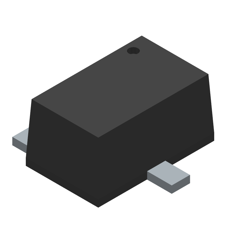
3D Model
Available Download Formats
By downloading CAD models, you agree to our Terms & Conditions and Privacy Policy
Small Signal Bipolar Transistor, 0.1A I(C), 50V V(BR)CEO, 1-Element, NPN, Silicon, HALOGEN FREE AND ROHS COMPLIANT, SMINI3-F2-B, SC-85, 3 PIN
Tip: Data for a part may vary between manufacturers. You can filter for manufacturers on the top of the page next to the part image and part number.
DRC5114W0L by Panasonic Electronic Components is a Small Signal Bipolar Transistor.
Small Signal Bipolar Transistors are under the broader part category of Transistors.
A transistor is a small semiconductor device used to amplify, control, or create electrical signals. When selecting a transistor, factors such as voltage, current rating, gain, and power dissipation must be considered, with common types. Read more about Transistors on our Transistors part category page.
By downloading CAD models, you agree to our Terms & Conditions and Privacy Policy
|
|
DRC5114W0L
Panasonic Electronic Components
Buy Now
Datasheet
|
Compare Parts:
DRC5114W0L
Panasonic Electronic Components
Small Signal Bipolar Transistor, 0.1A I(C), 50V V(BR)CEO, 1-Element, NPN, Silicon, HALOGEN FREE AND ROHS COMPLIANT, SMINI3-F2-B, SC-85, 3 PIN
|
| Rohs Code | Yes | |
| Part Life Cycle Code | Transferred | |
| Ihs Manufacturer | PANASONIC CORP | |
| Package Description | HALOGEN FREE AND ROHS COMPLIANT, SMINI3-F2-B, SC-85, 3 PIN | |
| Reach Compliance Code | unknown | |
| ECCN Code | EAR99 | |
| Samacsys Manufacturer | Panasonic | |
| Additional Feature | BUILT IN BIAS RESISTOR RATIO IS 0.47 | |
| Collector Current-Max (IC) | 0.1 A | |
| Collector-Emitter Voltage-Max | 50 V | |
| Configuration | SINGLE WITH BUILT-IN RESISTOR | |
| DC Current Gain-Min (hFE) | 20 | |
| JESD-30 Code | R-PDSO-F3 | |
| Number of Elements | 1 | |
| Number of Terminals | 3 | |
| Package Body Material | PLASTIC/EPOXY | |
| Package Shape | RECTANGULAR | |
| Package Style | SMALL OUTLINE | |
| Peak Reflow Temperature (Cel) | NOT SPECIFIED | |
| Polarity/Channel Type | NPN | |
| Surface Mount | YES | |
| Terminal Form | FLAT | |
| Terminal Position | DUAL | |
| Time@Peak Reflow Temperature-Max (s) | NOT SPECIFIED | |
| Transistor Application | SWITCHING | |
| Transistor Element Material | SILICON |
Panasonic recommends a 4-layer PCB with a solid ground plane, and a separate power plane for the input and output. The datasheet provides a recommended PCB layout, but it's essential to follow good PCB design practices, such as minimizing trace lengths and using adequate decoupling capacitors.
To ensure reliability in high-temperature applications, follow Panasonic's recommended derating guidelines for the device. Additionally, ensure good thermal management by providing adequate heat sinking and airflow. It's also essential to follow proper soldering and assembly techniques to prevent thermal stress on the device.
While the datasheet specifies the recommended operating voltage range, it's essential to note that the absolute maximum voltage ratings for the input and output pins are 6.5V and 5.5V, respectively. Exceeding these ratings can cause permanent damage to the device.
To troubleshoot issues with the DRC5114W0L, start by verifying the input voltage, output load, and PCB layout. Check for any signs of overheating, and ensure that the device is properly soldered and assembled. Use an oscilloscope to monitor the output voltage and current, and consult Panasonic's application notes and technical support resources for guidance.
Yes, the DRC5114W0L is a switching regulator, and as such, it can generate electromagnetic interference (EMI). To minimize EMI, follow good PCB design practices, such as using a solid ground plane, minimizing trace lengths, and using adequate shielding. Additionally, ensure that the device is properly decoupled, and consider using EMI filters or shielding components if necessary.