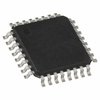
Part Details for CY29946AXI by Cypress Semiconductor
Results Overview of CY29946AXI by Cypress Semiconductor
- Distributor Offerings: (0 listings)
- Number of FFF Equivalents: (3 replacements)
- CAD Models: (Request Part)
- Number of Functional Equivalents: (10 options)
- Part Data Attributes: (Available)
- Reference Designs: (Not Available)
Tip: Data for a part may vary between manufacturers. You can filter for manufacturers on the top of the page next to the part image and part number.
CY29946AXI Information
CY29946AXI by Cypress Semiconductor is a Clock Driver.
Clock Drivers are under the broader part category of Logic Components.
Digital logic governs the behavior of signals in electronic circuits, enabling complex decisions based on simple binary inputs (yes/no). Logic components perform operations from these signals. Read more about Logic Components on our Logic part category page.
Part Details for CY29946AXI
CY29946AXI CAD Models
CY29946AXI Part Data Attributes
|
|
CY29946AXI
Cypress Semiconductor
Buy Now
Datasheet
|
Compare Parts:
CY29946AXI
Cypress Semiconductor
Low Skew Clock Driver, 29946 Series, 10 True Output(s), 0 Inverted Output(s), PQFP32, TQFP-32
|
| Pbfree Code | Yes | |
| Rohs Code | Yes | |
| Part Life Cycle Code | Obsolete | |
| Ihs Manufacturer | CYPRESS SEMICONDUCTOR CORP | |
| Part Package Code | QFP | |
| Package Description | TQFP-32 | |
| Pin Count | 32 | |
| Reach Compliance Code | compliant | |
| HTS Code | 8542.39.00.01 | |
| Additional Feature | IT CAN ALSO OPERATES AT 3.3V SUPPLY | |
| Family | 29946 | |
| Input Conditioning | DIFFERENTIAL MUX | |
| JESD-30 Code | S-PQFP-G32 | |
| JESD-609 Code | e3 | |
| Length | 7 mm | |
| Logic IC Type | LOW SKEW CLOCK DRIVER | |
| Max I(ol) | 0.02 A | |
| Moisture Sensitivity Level | 3 | |
| Number of Functions | 1 | |
| Number of Inverted Outputs | ||
| Number of Terminals | 32 | |
| Number of True Outputs | 10 | |
| Operating Temperature-Max | 85 °C | |
| Operating Temperature-Min | -40 °C | |
| Output Characteristics | 3-STATE | |
| Package Body Material | PLASTIC/EPOXY | |
| Package Code | TQFP | |
| Package Equivalence Code | TQFP32,.35SQ,32 | |
| Package Shape | SQUARE | |
| Package Style | FLATPACK, THIN PROFILE | |
| Peak Reflow Temperature (Cel) | 260 | |
| Prop. Delay@Nom-Sup | 11.5 ns | |
| Propagation Delay (tpd) | 11.5 ns | |
| Qualification Status | Not Qualified | |
| Same Edge Skew-Max (tskwd) | 0.25 ns | |
| Seated Height-Max | 1.2 mm | |
| Supply Voltage-Max (Vsup) | 2.625 V | |
| Supply Voltage-Min (Vsup) | 2.375 V | |
| Supply Voltage-Nom (Vsup) | 2.5 V | |
| Surface Mount | YES | |
| Temperature Grade | INDUSTRIAL | |
| Terminal Finish | MATTE TIN | |
| Terminal Form | GULL WING | |
| Terminal Pitch | 0.8 mm | |
| Terminal Position | QUAD | |
| Time@Peak Reflow Temperature-Max (s) | 20 | |
| Width | 7 mm |
Alternate Parts for CY29946AXI
This table gives cross-reference parts and alternative options found for CY29946AXI. The Form Fit Function (FFF) tab will give you the options that are more likely to serve as direct pin-to-pin alternates or drop-in parts. The Functional Equivalents tab will give you options that are likely to match the same function of CY29946AXI, but it may not fit your design. Always verify details of parts you are evaluating, as these parts are offered as suggestions for what you are looking for and are not guaranteed.
| Part Number | Manufacturer | Composite Price | Description | Compare |
|---|---|---|---|---|
| CY29946AI | Cypress Semiconductor | Check for Price | Low Skew Clock Driver, 10 True Output(s), 0 Inverted Output(s), PQFP32, 7 X 7 MM, 1 MM HEIGHT, PLASTIC, TQFP-32 | CY29946AXI vs CY29946AI |
| CY29946AIXT | Cypress Semiconductor | Check for Price | Low Skew Clock Driver, 29946 Series, 10 True Output(s), 0 Inverted Output(s), PQFP32, 7 X 7 MM, 1 MM HEIGHT, PLASTIC, TQFP-32 | CY29946AXI vs CY29946AIXT |
| CY29946AIT | Cypress Semiconductor | Check for Price | Low Skew Clock Driver, 10 True Output(s), 0 Inverted Output(s), PQFP32, 7 X 7 MM, 1 MM HEIGHT, PLASTIC, TQFP-32 | CY29946AXI vs CY29946AIT |
CY29946AXI Frequently Asked Questions (FAQ)
-
The recommended power-up sequence is to apply VCC first, followed by VCCIO, and then the clock signal. This ensures proper initialization and prevents latch-up conditions.
-
To configure the CY29946AXI for DDR3 memory interface, set the MRS (Memory Reference Signal) pin to '1' and use the DDR3-specific settings for the memory controller. Refer to the Cypress Semiconductor application note AN54427 for detailed configuration guidelines.
-
The CY29946AXI supports frequencies up to 133 MHz, but the actual frequency limit depends on the specific application, PCB design, and signal integrity. It's recommended to consult the datasheet and perform signal integrity analysis to determine the maximum frequency for your specific design.
-
To implement clock domain crossing with the CY29946AXI, use the built-in CDC logic and follow the guidelines provided in the Cypress Semiconductor application note AN54427. This includes using the CDC registers, synchronizing clock domains, and ensuring proper metastability resolution.
-
The JTAG pins on the CY29946AXI are used for boundary scan testing, debugging, and programming. They allow for access to the device's internal registers and facilitate debugging and testing of the device and the surrounding circuitry.
