-
Part Symbol
-
Footprint
-
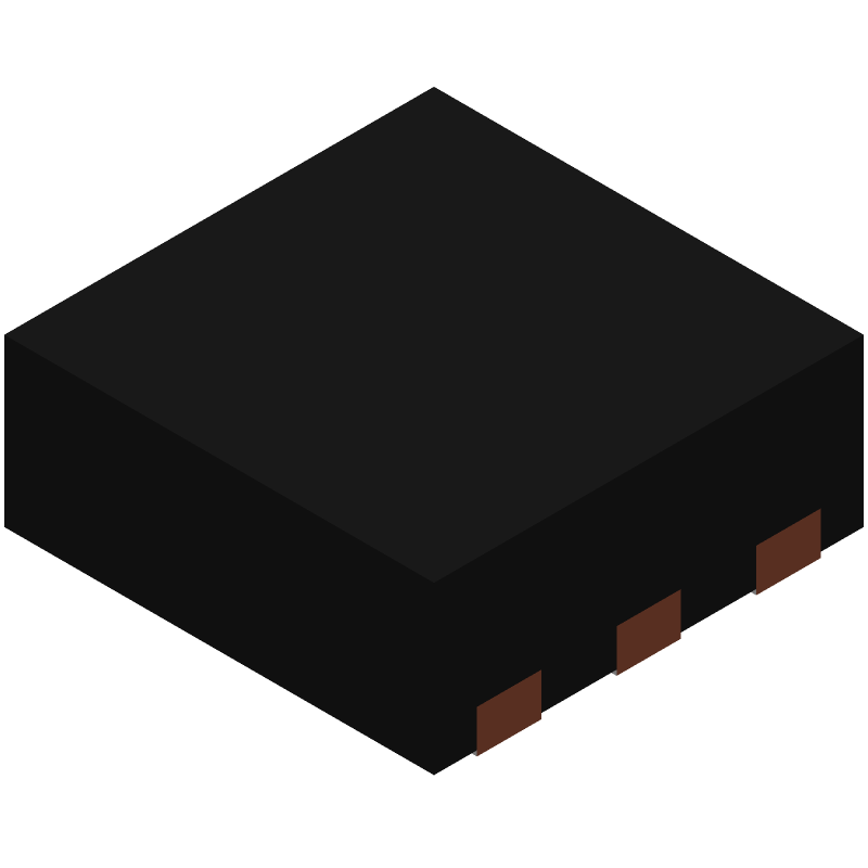
3D Model
Available Download Formats
By downloading CAD models, you agree to our Terms & Conditions and Privacy Policy
P-Channel NexFET™ Power MOSFET 6-WSON -55 to 150
Tip: Data for a part may vary between manufacturers. You can filter for manufacturers on the top of the page next to the part image and part number.
CSD25302Q2 by Texas Instruments is a Power Field-Effect Transistor.
Power Field-Effect Transistors are under the broader part category of Transistors.
A transistor is a small semiconductor device used to amplify, control, or create electrical signals. When selecting a transistor, factors such as voltage, current rating, gain, and power dissipation must be considered, with common types. Read more about Transistors on our Transistors part category page.
| Part # | Distributor | Description | Stock | Price | Buy | |
|---|---|---|---|---|---|---|
|
|
Bristol Electronics | 131 |
|
RFQ | ||
|
|
Vyrian | Peripheral ICs | 687 |
|
RFQ |
By downloading CAD models, you agree to our Terms & Conditions and Privacy Policy
|
|
CSD25302Q2
Texas Instruments
Buy Now
Datasheet
|
Compare Parts:
CSD25302Q2
Texas Instruments
P-Channel NexFET™ Power MOSFET 6-WSON -55 to 150
|
| Pbfree Code | No | |
| Rohs Code | Yes | |
| Part Life Cycle Code | Obsolete | |
| Ihs Manufacturer | TEXAS INSTRUMENTS INC | |
| Package Description | SON-6 | |
| Pin Count | 6 | |
| Reach Compliance Code | unknown | |
| ECCN Code | EAR99 | |
| Samacsys Manufacturer | Texas Instruments | |
| Additional Feature | AVALANCHE RATED | |
| Case Connection | SOURCE | |
| Configuration | SINGLE WITH BUILT-IN DIODE | |
| DS Breakdown Voltage-Min | 20 V | |
| Drain Current-Max (ID) | 5 A | |
| Drain-source On Resistance-Max | 0.092 Ω | |
| FET Technology | METAL-OXIDE SEMICONDUCTOR | |
| JESD-30 Code | S-PDSO-N6 | |
| JESD-609 Code | e3 | |
| Moisture Sensitivity Level | 1 | |
| Number of Elements | 1 | |
| Number of Terminals | 6 | |
| Operating Mode | ENHANCEMENT MODE | |
| Operating Temperature-Max | 150 °C | |
| Package Body Material | PLASTIC/EPOXY | |
| Package Shape | SQUARE | |
| Package Style | SMALL OUTLINE | |
| Peak Reflow Temperature (Cel) | 260 | |
| Polarity/Channel Type | P-CHANNEL | |
| Power Dissipation-Max (Abs) | 2.4 W | |
| Pulsed Drain Current-Max (IDM) | 20 A | |
| Qualification Status | Not Qualified | |
| Surface Mount | YES | |
| Terminal Finish | MATTE TIN | |
| Terminal Form | NO LEAD | |
| Terminal Position | DUAL | |
| Time@Peak Reflow Temperature-Max (s) | 30 | |
| Transistor Application | SWITCHING | |
| Transistor Element Material | SILICON |
This table gives cross-reference parts and alternative options found for CSD25302Q2. The Form Fit Function (FFF) tab will give you the options that are more likely to serve as direct pin-to-pin alternates or drop-in parts. The Functional Equivalents tab will give you options that are likely to match the same function of CSD25302Q2, but it may not fit your design. Always verify details of parts you are evaluating, as these parts are offered as suggestions for what you are looking for and are not guaranteed.
| Part Number | Manufacturer | Composite Price | Description | Compare |
|---|---|---|---|---|
| TSM301K12CQRFG | Taiwan Semiconductor | Check for Price | Power Field-Effect Transistor, | CSD25302Q2 vs TSM301K12CQRFG |
A good PCB layout for CSD25302Q2 involves keeping the high-current paths short and wide, using multiple vias for thermal relief, and placing the device near the power source to minimize inductance. A 2-layer or 4-layer board is recommended, with the device on the top layer and the power plane on the inner layer.
Proper thermal management involves attaching a heat sink to the device, using thermal interface material (TIM) to fill gaps, and ensuring good airflow around the device. The heat sink should be designed to handle the maximum power dissipation of the device, and the thermal resistance of the system should be minimized.
When selecting input capacitors for CSD25302Q2, consider the voltage rating, capacitance value, and equivalent series resistance (ESR). The capacitor should be rated for the maximum input voltage, and the capacitance value should be sufficient to filter out ripple and noise. A low ESR is essential to minimize power losses.
To troubleshoot issues with CSD25302Q2, start by checking the input voltage, output voltage, and current. Verify that the device is properly soldered and that the PCB layout is correct. Check for signs of overheating, such as excessive temperature or thermal shutdown. Use oscilloscopes and current probes to measure waveforms and currents, and consult the datasheet and application notes for guidance.
The CSD25302Q2 is a high-current, low-voltage synchronous buck converter with a unique feature set, including a wide input voltage range and high efficiency. Compared to other devices, it has a higher current rating, faster switching frequency, and a more comprehensive set of protection features. Consult the datasheet and product page for a detailed comparison with other devices.