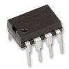
Part Details for CPC5902G by IXYS Corporation
Results Overview of CPC5902G by IXYS Corporation
- Distributor Offerings: (1 listing)
- Number of FFF Equivalents: (0 replacements)
- CAD Models: (Request Part)
- Number of Functional Equivalents: (0 options)
- Part Data Attributes: (Available)
- Reference Designs: (Not Available)
Tip: Data for a part may vary between manufacturers. You can filter for manufacturers on the top of the page next to the part image and part number.
CPC5902G Information
CPC5902G by IXYS Corporation is an Other Signal Circuit.
Other Signal Circuits are under the broader part category of Signal Circuits.
A signal is an electronic means of transmitting information, either as an analog signal with continuous values or a digital signal with discrete values. Signals are used in various systems and networks. Read more about Signal Circuits on our Signal Circuits part category page.
Price & Stock for CPC5902G
| Part # | Distributor | Description | Stock | Price | Buy | |
|---|---|---|---|---|---|---|
|
|
New Advantage Corporation | IC-5902 OPTOISO BUS REPEATER DIP8 RoHS: Compliant Min Qty: 1 Package Multiple: 100 | 611 |
|
$9.3600 / $10.1300 | Buy Now |
Part Details for CPC5902G
CPC5902G CAD Models
CPC5902G Part Data Attributes
|
|
CPC5902G
IXYS Corporation
Buy Now
Datasheet
|
Compare Parts:
CPC5902G
IXYS Corporation
Analog Circuit, 1 Func, PDIP8, DIP-8
|
| Rohs Code | Yes | |
| Part Life Cycle Code | Obsolete | |
| Ihs Manufacturer | IXYS CORP | |
| Part Package Code | DIP | |
| Package Description | DIP-8 | |
| Pin Count | 8 | |
| Reach Compliance Code | compliant | |
| HTS Code | 8542.39.00.01 | |
| Additional Feature | SEATED HGT-NOM | |
| Analog IC - Other Type | ANALOG CIRCUIT | |
| JESD-30 Code | R-PDIP-T8 | |
| Length | 9.652 mm | |
| Number of Functions | 1 | |
| Number of Terminals | 8 | |
| Operating Temperature-Max | 85 °C | |
| Operating Temperature-Min | -40 °C | |
| Package Body Material | PLASTIC/EPOXY | |
| Package Code | DIP | |
| Package Shape | RECTANGULAR | |
| Package Style | IN-LINE | |
| Peak Reflow Temperature (Cel) | 250 | |
| Seated Height-Max | 4.064 mm | |
| Supply Voltage-Max (Vsup) | 5.5 V | |
| Supply Voltage-Min (Vsup) | 2.7 V | |
| Supply Voltage-Nom (Vsup) | 3.3 V | |
| Surface Mount | NO | |
| Temperature Grade | INDUSTRIAL | |
| Terminal Form | THROUGH-HOLE | |
| Terminal Pitch | 2.54 mm | |
| Terminal Position | DUAL | |
| Time@Peak Reflow Temperature-Max (s) | 10 | |
| Width | 7.62 mm |
CPC5902G Frequently Asked Questions (FAQ)
-
The recommended PCB layout for optimal thermal performance involves placing the device on a thermal pad with a minimum size of 1 inch x 1 inch, and using multiple vias to connect the thermal pad to a solid copper plane on the bottom layer of the PCB. This helps to dissipate heat efficiently and reduce thermal resistance.
-
To ensure reliable operation in high-temperature environments, it is recommended to derate the device's power handling capability according to the temperature derating curve provided in the datasheet. Additionally, ensure good thermal design and heat sinking to keep the device junction temperature below the maximum rated value.
-
The recommended gate drive circuit for CPC5902G involves using a gate driver IC with a high current capability (e.g. IX4420) and a gate resistor (e.g. 10 ohms) to ensure fast switching times and minimize ringing. The gate drive voltage should be set to 15V to ensure reliable turn-on and turn-off.
-
To protect the device from overvoltage and overcurrent conditions, it is recommended to use a voltage clamp circuit (e.g. a zener diode and a resistor) to limit the voltage across the device, and a current sense resistor to monitor the current through the device. Additionally, consider using a fuse or a current limiter to prevent excessive current flow.
-
The recommended storage and handling procedure for CPC5902G involves storing the devices in their original packaging or in a dry, ESD-protected environment. Avoid touching the device pins or exposing them to moisture, and handle the devices by the body only to prevent ESD damage.
