-
Part Symbol
-
Footprint
-
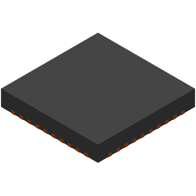
3D Model
Available Download Formats
By downloading CAD models, you agree to our Terms & Conditions and Privacy Policy

Low jitter, 2-input selectable 1:12 universal-to-LVDS buffer 40-VQFN -40 to 85
Tip: Data for a part may vary between manufacturers. You can filter for manufacturers on the top of the page next to the part image and part number.
CDCLVD1212RHAR by Texas Instruments is a Clock Driver.
Clock Drivers are under the broader part category of Logic Components.
Digital logic governs the behavior of signals in electronic circuits, enabling complex decisions based on simple binary inputs (yes/no). Logic components perform operations from these signals. Read more about Logic Components on our Logic part category page.
| Part # | Distributor | Description | Stock | Price | Buy | |
|---|---|---|---|---|---|---|
|
DISTI #
296-48508-1-ND
|
DigiKey | IC CLK BUFFER 2:12 800MHZ 40VQFN Min Qty: 1 Lead time: 6 Weeks Container: Cut Tape (CT), Digi-Reel®, Tape & Reel (TR) |
758 In Stock |
|
$4.7109 / $8.1300 | Buy Now |
|
DISTI #
595-CDCLVD1212RHAR
|
Mouser Electronics | Clock Buffer Low Jitter 2-Inp Sel 1:12 Uni-to-LVDS Bf A 595-CDCLVD1212RHAT RoHS: Compliant | 2521 |
|
$4.8100 / $8.1300 | Buy Now |
|
DISTI #
SMC-CDCLVD1212RHAR
|
Sensible Micro Corporation | AS6081 Certified Vendor, 1 Yr Warranty RoHS: Not Compliant Min Qty: 25 Lead time: 2 Weeks, 0 Days | 2643 |
|
RFQ | |
|
|
Velocity Electronics | Our Stock | 3 |
|
RFQ | |
|
|
Vyrian | Logic ICs | 3482 |
|
RFQ | |
|
|
Win Source Electronics | IC CLK BUFFER 2:12 800MHZ 40VQFN | 3900 |
|
$7.2083 / $9.3106 | Buy Now |
By downloading CAD models, you agree to our Terms & Conditions and Privacy Policy
|
|
CDCLVD1212RHAR
Texas Instruments
Buy Now
Datasheet
|
Compare Parts:
CDCLVD1212RHAR
Texas Instruments
Low jitter, 2-input selectable 1:12 universal-to-LVDS buffer 40-VQFN -40 to 85
|
| Pbfree Code | Yes | |
| Rohs Code | Yes | |
| Part Life Cycle Code | Active | |
| Ihs Manufacturer | TEXAS INSTRUMENTS INC | |
| Part Package Code | QFN | |
| Package Description | 6 X 6 MM, PLASTIC, MO-220VJJD-2, VQFN-40 | |
| Pin Count | 40 | |
| Reach Compliance Code | compliant | |
| ECCN Code | EAR99 | |
| HTS Code | 8542.39.00.01 | |
| Samacsys Manufacturer | Texas Instruments | |
| Family | CDC | |
| Input Conditioning | MUX | |
| JESD-30 Code | S-PQCC-N40 | |
| JESD-609 Code | e4 | |
| Length | 6 mm | |
| Logic IC Type | LOW SKEW CLOCK DRIVER | |
| Moisture Sensitivity Level | 3 | |
| Number of Functions | 1 | |
| Number of Inverted Outputs | ||
| Number of Terminals | 40 | |
| Number of True Outputs | 12 | |
| Operating Temperature-Max | 85 °C | |
| Operating Temperature-Min | -40 °C | |
| Package Body Material | PLASTIC/EPOXY | |
| Package Code | HVQCCN | |
| Package Equivalence Code | LCC40,.24SQ,20 | |
| Package Shape | SQUARE | |
| Package Style | CHIP CARRIER, HEAT SINK/SLUG, VERY THIN PROFILE | |
| Packing Method | TR | |
| Peak Reflow Temperature (Cel) | 260 | |
| Prop. Delay@Nom-Sup | 2.5 ns | |
| Propagation Delay (tpd) | 2.5 ns | |
| Qualification Status | Not Qualified | |
| Same Edge Skew-Max (tskwd) | 0.05 ns | |
| Seated Height-Max | 1 mm | |
| Supply Voltage-Max (Vsup) | 2.625 V | |
| Supply Voltage-Min (Vsup) | 2.375 V | |
| Supply Voltage-Nom (Vsup) | 2.5 V | |
| Surface Mount | YES | |
| Temperature Grade | INDUSTRIAL | |
| Terminal Finish | Nickel/Palladium/Gold (Ni/Pd/Au) | |
| Terminal Form | NO LEAD | |
| Terminal Pitch | 0.5 mm | |
| Terminal Position | QUAD | |
| Time@Peak Reflow Temperature-Max (s) | 30 | |
| Width | 6 mm | |
| fmax-Min | 800 MHz |
This table gives cross-reference parts and alternative options found for CDCLVD1212RHAR. The Form Fit Function (FFF) tab will give you the options that are more likely to serve as direct pin-to-pin alternates or drop-in parts. The Functional Equivalents tab will give you options that are likely to match the same function of CDCLVD1212RHAR, but it may not fit your design. Always verify details of parts you are evaluating, as these parts are offered as suggestions for what you are looking for and are not guaranteed.
| Part Number | Manufacturer | Composite Price | Description | Compare |
|---|---|---|---|---|
| CDCLVD1212RHAT | Texas Instruments | $4.5381 | Low jitter, 2-input selectable 1:12 universal-to-LVDS buffer 40-VQFN -40 to 85 | CDCLVD1212RHAR vs CDCLVD1212RHAT |
| 8SLVD1212NLGI/W | Integrated Device Technology Inc | Check for Price | VFQFPN-40, Reel | CDCLVD1212RHAR vs 8SLVD1212NLGI/W |
| 8SLVD1212ANLGI8 | Renesas Electronics Corporation | Check for Price | 1:12, LVDS Output Fanout Buffer, VFQFPN0/Reel | CDCLVD1212RHAR vs 8SLVD1212ANLGI8 |
| 8SLVD1212ANLGI8 | Integrated Device Technology Inc | Check for Price | VFQFPN-40, Reel | CDCLVD1212RHAR vs 8SLVD1212ANLGI8 |
| 8SLVD1212NLGI8 | Integrated Device Technology Inc | Check for Price | VFQFPN-40, Reel | CDCLVD1212RHAR vs 8SLVD1212NLGI8 |
Texas Instruments recommends a symmetrical layout, with the device placed near the center of the board, and using a solid ground plane to reduce noise. Additionally, use short, direct traces for clock signals, and avoid crossing clock signals with other signals.
Use a series termination resistor (Rs) of 50-75 ohms, and a parallel termination capacitor (Cp) of 1-2 pF, placed close to the output pin. This will help match the impedance and reduce signal reflection.
The maximum frequency deviation for the input clock signal is ±100 ppm. If the input clock signal deviates beyond this range, it may affect the output clock signal's frequency, phase, and jitter performance.
The CDCLVD1212RHAR can tolerate input clock signal duty cycle distortion up to 45/55%. However, excessive distortion may affect the output clock signal's duty cycle, and may require additional conditioning or correction.
Use a 10-22 uF decoupling capacitor, placed close to the power pin, and a 1-10 uF filter capacitor, placed between the power pin and ground. This will help reduce power supply noise and jitter.