-
Part Symbol
-
Footprint
-
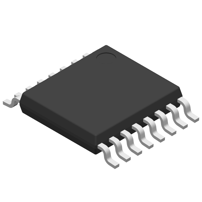
3D Model
Available Download Formats
By downloading CAD models, you agree to our Terms & Conditions and Privacy Policy

Low jitter, 1:8 LVCMOS fan-out clock buffer 16-TSSOP -40 to 85
Tip: Data for a part may vary between manufacturers. You can filter for manufacturers on the top of the page next to the part image and part number.
CDCLVC1108PWR by Texas Instruments is a Clock Driver.
Clock Drivers are under the broader part category of Logic Components.
Digital logic governs the behavior of signals in electronic circuits, enabling complex decisions based on simple binary inputs (yes/no). Logic components perform operations from these signals. Read more about Logic Components on our Logic part category page.
| Part # | Distributor | Description | Stock | Price | Buy | |
|---|---|---|---|---|---|---|
|
DISTI #
296-27589-1-ND
|
DigiKey | IC CLK BUFFER 1:8 250MHZ 16TSSOP Min Qty: 1 Lead time: 6 Weeks Container: Digi-Reel®, Cut Tape (CT), Tape & Reel (TR) |
2125 In Stock |
|
$2.2352 / $4.1500 | Buy Now |
|
DISTI #
595-CDCLVC1108PWR
|
Mouser Electronics | Clock Buffer Lo Jitter 1:8 LVCMOS Fan-out Clock Bfr A 595-CDCLVC1108PW RoHS: Compliant | 3024 |
|
$2.3300 / $4.1500 | Buy Now |
|
|
Bristol Electronics | 161 |
|
RFQ | ||
|
|
Quest Components | LOW SKEW CLOCK DRIVER, CDC SERIES, 1 TRUE OUTPUT(S), 0 INVERTED OUTPUT(S), CMOS, PDSO16 | 128 |
|
$5.5500 / $9.0000 | Buy Now |
|
DISTI #
SMC-CDCLVC1108PWR
|
Sensible Micro Corporation | AS6081 Certified Vendor, 1 Yr Warranty RoHS: Not Compliant Min Qty: 25 Lead time: 2 Weeks, 0 Days | 4000 |
|
RFQ |
By downloading CAD models, you agree to our Terms & Conditions and Privacy Policy
|
|
CDCLVC1108PWR
Texas Instruments
Buy Now
Datasheet
|
Compare Parts:
CDCLVC1108PWR
Texas Instruments
Low jitter, 1:8 LVCMOS fan-out clock buffer 16-TSSOP -40 to 85
|
| Pbfree Code | Yes | |
| Rohs Code | Yes | |
| Part Life Cycle Code | Active | |
| Ihs Manufacturer | TEXAS INSTRUMENTS INC | |
| Part Package Code | TSSOP | |
| Package Description | TSSOP-16 | |
| Pin Count | 16 | |
| Reach Compliance Code | compliant | |
| ECCN Code | EAR99 | |
| HTS Code | 8542.39.00.01 | |
| Samacsys Manufacturer | Texas Instruments | |
| Family | CDC | |
| Input Conditioning | STANDARD | |
| JESD-30 Code | R-PDSO-G16 | |
| JESD-609 Code | e4 | |
| Length | 5 mm | |
| Logic IC Type | LOW SKEW CLOCK DRIVER | |
| Max I(ol) | 0.012 A | |
| Moisture Sensitivity Level | 1 | |
| Number of Functions | 1 | |
| Number of Inverted Outputs | ||
| Number of Terminals | 16 | |
| Number of True Outputs | 1 | |
| Operating Temperature-Max | 85 °C | |
| Operating Temperature-Min | -40 °C | |
| Output Characteristics | 3-STATE | |
| Package Body Material | PLASTIC/EPOXY | |
| Package Code | TSSOP | |
| Package Equivalence Code | TSSOP16,.25 | |
| Package Shape | RECTANGULAR | |
| Package Style | SMALL OUTLINE | |
| Packing Method | TR | |
| Peak Reflow Temperature (Cel) | 260 | |
| Prop. Delay@Nom-Sup | 2 ns | |
| Propagation Delay (tpd) | 2.6 ns | |
| Qualification Status | Not Qualified | |
| Same Edge Skew-Max (tskwd) | 0.05 ns | |
| Seated Height-Max | 1.2 mm | |
| Supply Voltage-Max (Vsup) | 2.7 V | |
| Supply Voltage-Min (Vsup) | 2.3 V | |
| Supply Voltage-Nom (Vsup) | 2.5 V | |
| Surface Mount | YES | |
| Technology | CMOS | |
| Temperature Grade | INDUSTRIAL | |
| Terminal Finish | Nickel/Palladium/Gold (Ni/Pd/Au) | |
| Terminal Form | GULL WING | |
| Terminal Pitch | 0.65 mm | |
| Terminal Position | DUAL | |
| Time@Peak Reflow Temperature-Max (s) | 30 | |
| Width | 4.4 mm | |
| fmax-Min | 250 MHz |
This table gives cross-reference parts and alternative options found for CDCLVC1108PWR. The Form Fit Function (FFF) tab will give you the options that are more likely to serve as direct pin-to-pin alternates or drop-in parts. The Functional Equivalents tab will give you options that are likely to match the same function of CDCLVC1108PWR, but it may not fit your design. Always verify details of parts you are evaluating, as these parts are offered as suggestions for what you are looking for and are not guaranteed.
| Part Number | Manufacturer | Composite Price | Description | Compare |
|---|---|---|---|---|
| CDCLVC1108PW | Texas Instruments | $2.7485 | Low jitter, 1:8 LVCMOS fan-out clock buffer 16-TSSOP -40 to 85 | CDCLVC1108PWR vs CDCLVC1108PW |
A good PCB layout for the CDCLVC1108PWR involves keeping the input and output traces short and away from each other, using a solid ground plane, and placing decoupling capacitors close to the device. TI provides a recommended layout in the datasheet and application notes.
To ensure proper power and decoupling, use a low-ESR capacitor (e.g., 0.1 μF) between VCC and GND, and a larger capacitor (e.g., 10 μF) between VCC and GND for bulk decoupling. Place these capacitors close to the device and use a low-inductance path to the power pins.
The CDCLVC1108PWR can operate up to 200 MHz, but the maximum frequency of operation depends on the specific application, output load, and clock signal quality. Consult the datasheet and application notes for more information.
Configure the CDCLVC1108PWR by selecting the appropriate input clock frequency, output frequency, and output format (e.g., LVCMOS, LVDS, or HCSL). Use the device's internal dividers and multipliers to generate the desired output frequency. Consult the datasheet and application notes for specific configuration examples.
The CDCLVC1108PWR has a maximum junction temperature of 150°C. Ensure good thermal conduction by using a heat sink or thermal pad, and avoid overheating by keeping the device within the recommended operating temperature range (–40°C to 85°C).