-
Part Symbol
-
Footprint
-
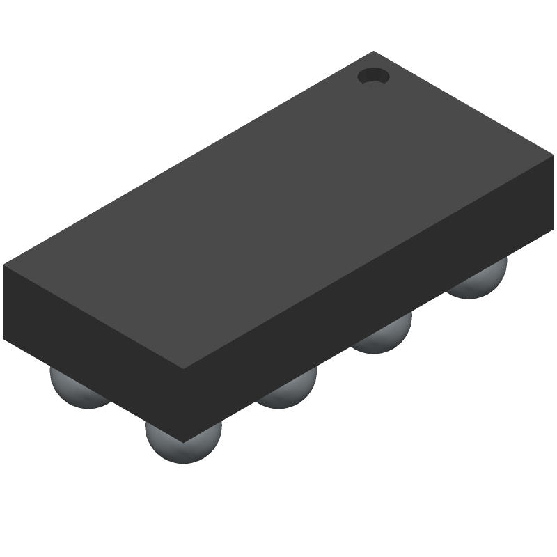
3D Model
Available Download Formats
By downloading CAD models, you agree to our Terms & Conditions and Privacy Policy

Dual-channel square/sine-to-square wave clock buffer 8-DSBGA -40 to 85
Tip: Data for a part may vary between manufacturers. You can filter for manufacturers on the top of the page next to the part image and part number.
CDC3RL02YFPR by Texas Instruments is a Clock Driver.
Clock Drivers are under the broader part category of Logic Components.
Digital logic governs the behavior of signals in electronic circuits, enabling complex decisions based on simple binary inputs (yes/no). Logic components perform operations from these signals. Read more about Logic Components on our Logic part category page.
| Part # | Distributor | Description | Stock | Price | Buy | |
|---|---|---|---|---|---|---|
|
DISTI #
296-25452-1-ND
|
DigiKey | IC CLK BUFFER 1:2 52MHZ 8DSBGA Min Qty: 1 Lead time: 6 Weeks Container: Digi-Reel®, Cut Tape (CT), Tape & Reel (TR) |
7206 In Stock |
|
$0.6930 / $1.4600 | Buy Now |
|
DISTI #
595-CDC3RL02YFPR
|
Mouser Electronics | Clock Buffer 2Ch Square/Sine- to- Square Wave Clock RoHS: Compliant | 3565 |
|
$0.6430 / $1.5400 | Buy Now |
|
|
Bristol Electronics | 2998 |
|
RFQ | ||
|
|
Bristol Electronics | 2263 |
|
RFQ | ||
|
|
Quest Components | CDC SERIES, LOW SKEW CLOCK DRIVER, 2 TRUE OUTPUT(S), 0 INVERTED OUTPUT(S), PBGA8 | 2398 |
|
$0.7910 / $2.1092 | Buy Now |
|
|
Quest Components | CDC SERIES, LOW SKEW CLOCK DRIVER, 2 TRUE OUTPUT(S), 0 INVERTED OUTPUT(S), PBGA8 | 2215 |
|
$0.5537 / $1.3183 | Buy Now |
|
|
Quest Components | CDC SERIES, LOW SKEW CLOCK DRIVER, 2 TRUE OUTPUT(S), 0 INVERTED OUTPUT(S), PBGA8 | 1724 |
|
$0.7910 / $2.1092 | Buy Now |
|
|
Quest Components | CDC SERIES, LOW SKEW CLOCK DRIVER, 2 TRUE OUTPUT(S), 0 INVERTED OUTPUT(S), PBGA8 | 183 |
|
$1.0546 / $2.1092 | Buy Now |
|
|
Quest Components | CDC SERIES, LOW SKEW CLOCK DRIVER, 2 TRUE OUTPUT(S), 0 INVERTED OUTPUT(S), PBGA8 | 51 |
|
$1.4914 / $2.7116 | Buy Now |
|
DISTI #
CDC3RL02YFPR
|
Chip One Stop | Semiconductors RoHS: Compliant pbFree: Yes Min Qty: 1 Lead time: 0 Weeks, 1 Days Container: Cut Tape | 2935 |
|
$0.6410 / $1.4000 | Buy Now |
By downloading CAD models, you agree to our Terms & Conditions and Privacy Policy
|
|
CDC3RL02YFPR
Texas Instruments
Buy Now
Datasheet
|
Compare Parts:
CDC3RL02YFPR
Texas Instruments
Dual-channel square/sine-to-square wave clock buffer 8-DSBGA -40 to 85
|
| Pbfree Code | Yes | |
| Rohs Code | Yes | |
| Part Life Cycle Code | Active | |
| Ihs Manufacturer | TEXAS INSTRUMENTS INC | |
| Part Package Code | BGA | |
| Package Description | WCSP-8 | |
| Pin Count | 8 | |
| Reach Compliance Code | compliant | |
| ECCN Code | EAR99 | |
| HTS Code | 8542.39.00.01 | |
| Samacsys Manufacturer | Texas Instruments | |
| Family | CDC | |
| Input Conditioning | STANDARD | |
| JESD-30 Code | R-PBGA-B8 | |
| JESD-609 Code | e1 | |
| Length | 1.57 mm | |
| Load Capacitance (CL) | 50 pF | |
| Logic IC Type | LOW SKEW CLOCK DRIVER | |
| Max I(ol) | 0.008 A | |
| Moisture Sensitivity Level | 1 | |
| Number of Functions | 1 | |
| Number of Inverted Outputs | ||
| Number of Terminals | 8 | |
| Number of True Outputs | 2 | |
| Operating Temperature-Max | 85 °C | |
| Operating Temperature-Min | -40 °C | |
| Package Body Material | PLASTIC/EPOXY | |
| Package Code | VFBGA | |
| Package Equivalence Code | BGA8,2X4,16 | |
| Package Shape | RECTANGULAR | |
| Package Style | GRID ARRAY, VERY THIN PROFILE, FINE PITCH | |
| Packing Method | TR | |
| Peak Reflow Temperature (Cel) | 260 | |
| Qualification Status | Not Qualified | |
| Seated Height-Max | 0.5 mm | |
| Supply Voltage-Max (Vsup) | 5.5 V | |
| Supply Voltage-Min (Vsup) | 2.3 V | |
| Supply Voltage-Nom (Vsup) | 1.8 V | |
| Surface Mount | YES | |
| Temperature Grade | INDUSTRIAL | |
| Terminal Finish | Tin/Silver/Copper (Sn/Ag/Cu) | |
| Terminal Form | BALL | |
| Terminal Pitch | 0.4 mm | |
| Terminal Position | BOTTOM | |
| Time@Peak Reflow Temperature-Max (s) | 30 | |
| Width | 0.77 mm | |
| fmax-Min | 52 MHz |
Texas Instruments recommends following a star topology for clock distribution, using a solid ground plane, and keeping clock traces short and matched in length to minimize jitter and ensure signal integrity.
The output frequency of the CDC3RL02YFPR depends on the input frequency and the desired output frequency. Use the frequency selection table in the datasheet to determine the correct output frequency for your application.
The CDC3RL02YFPR can handle input frequencies up to 200 MHz, but the maximum input frequency may vary depending on the specific application and operating conditions.
Use a low-ESR capacitor (e.g., 0.1 μF) to decouple the power supply, and ensure that the power supply voltage is within the recommended range (1.8 V to 3.6 V).
The typical power consumption of the CDC3RL02YFPR is around 10 mA, but this can vary depending on the input frequency, output frequency, and operating conditions.