-
Part Symbol
-
Footprint
-
3D Model
Available Download Formats
By downloading CAD models, you agree to our Terms & Conditions and Privacy Policy

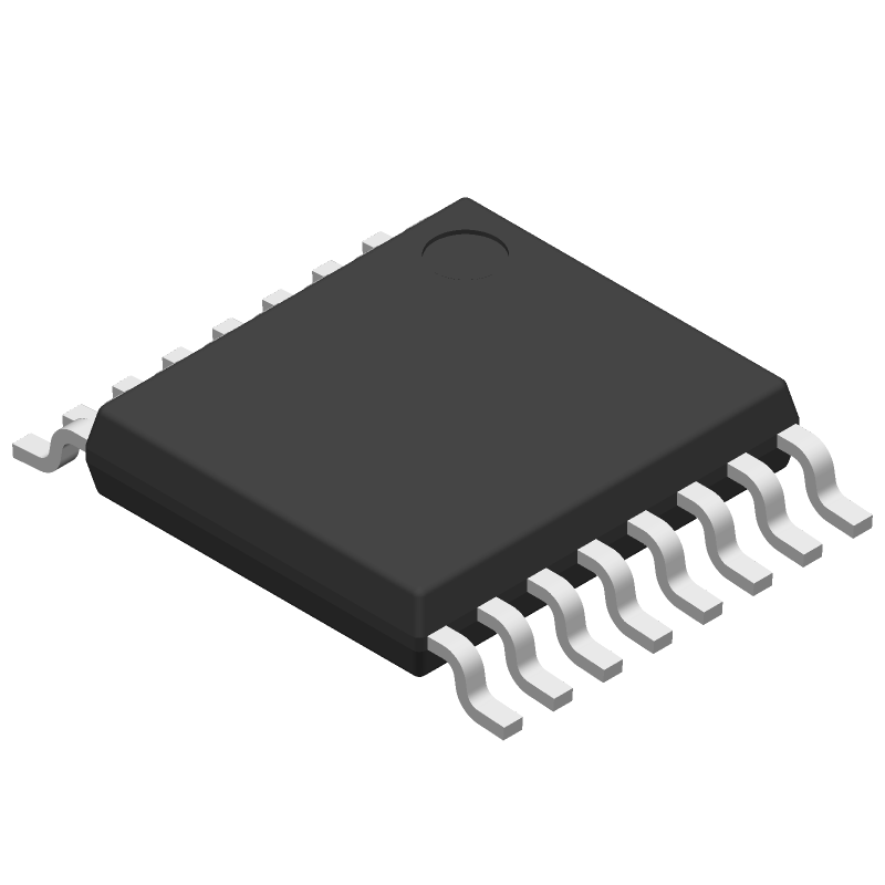
CMOS BCD-to-7-Segment LED Latch Decoder Drivers 16-TSSOP -55 to 125
Tip: Data for a part may vary between manufacturers. You can filter for manufacturers on the top of the page next to the part image and part number.
CD4511BPWG4 by Texas Instruments is a Decoder/Driver.
Decoder/Drivers are under the broader part category of Logic Components.
Digital logic governs the behavior of signals in electronic circuits, enabling complex decisions based on simple binary inputs (yes/no). Logic components perform operations from these signals. Read more about Logic Components on our Logic part category page.
| Part # | Distributor | Description | Stock | Price | Buy | |
|---|---|---|---|---|---|---|
|
|
Vyrian | Logic ICs | 254 |
|
RFQ |
By downloading CAD models, you agree to our Terms & Conditions and Privacy Policy
|
|
CD4511BPWG4
Texas Instruments
Buy Now
Datasheet
|
Compare Parts:
CD4511BPWG4
Texas Instruments
CMOS BCD-to-7-Segment LED Latch Decoder Drivers 16-TSSOP -55 to 125
|
| Rohs Code | Yes | |
| Part Life Cycle Code | Obsolete | |
| Ihs Manufacturer | TEXAS INSTRUMENTS INC | |
| Part Package Code | TSSOP | |
| Package Description | TSSOP-16 | |
| Pin Count | 16 | |
| Reach Compliance Code | compliant | |
| ECCN Code | EAR99 | |
| HTS Code | 8542.39.00.01 | |
| Samacsys Manufacturer | Texas Instruments | |
| Family | 4000/14000/40000 | |
| Input Conditioning | LATCHED | |
| JESD-30 Code | R-PDSO-G16 | |
| JESD-609 Code | e4 | |
| Length | 5 mm | |
| Load Capacitance (CL) | 50 pF | |
| Logic IC Type | SEVEN SEGMENT DECODER/DRIVER | |
| Max I(ol) | 0.0015 A | |
| Moisture Sensitivity Level | 1 | |
| Number of Functions | 1 | |
| Number of Terminals | 16 | |
| Operating Temperature-Max | 125 °C | |
| Operating Temperature-Min | -55 °C | |
| Output Polarity | TRUE | |
| Package Body Material | PLASTIC/EPOXY | |
| Package Code | TSSOP | |
| Package Equivalence Code | TSSOP16,.25 | |
| Package Shape | RECTANGULAR | |
| Package Style | SMALL OUTLINE, THIN PROFILE, SHRINK PITCH | |
| Packing Method | TUBE | |
| Peak Reflow Temperature (Cel) | 260 | |
| Power Supply Current-Max (ICC) | 3 mA | |
| Prop. Delay@Nom-Sup | 420 ns | |
| Propagation Delay (tpd) | 1320 ns | |
| Qualification Status | Not Qualified | |
| Seated Height-Max | 1.2 mm | |
| Supply Voltage-Max (Vsup) | 18 V | |
| Supply Voltage-Min (Vsup) | 3 V | |
| Supply Voltage-Nom (Vsup) | 5 V | |
| Surface Mount | YES | |
| Technology | CMOS | |
| Temperature Grade | MILITARY | |
| Terminal Finish | NICKEL PALLADIUM GOLD | |
| Terminal Form | GULL WING | |
| Terminal Pitch | 0.65 mm | |
| Terminal Position | DUAL | |
| Time@Peak Reflow Temperature-Max (s) | 30 | |
| Width | 4.4 mm |
This table gives cross-reference parts and alternative options found for CD4511BPWG4. The Form Fit Function (FFF) tab will give you the options that are more likely to serve as direct pin-to-pin alternates or drop-in parts. The Functional Equivalents tab will give you options that are likely to match the same function of CD4511BPWG4, but it may not fit your design. Always verify details of parts you are evaluating, as these parts are offered as suggestions for what you are looking for and are not guaranteed.
| Part Number | Manufacturer | Composite Price | Description | Compare |
|---|---|---|---|---|
| CD4511BPWR | Texas Instruments | $0.1768 | CMOS BCD-to-7-Segment LED Latch Decoder Drivers 16-TSSOP -55 to 125 | CD4511BPWG4 vs CD4511BPWR |
| CD4511BPWE4 | Texas Instruments | Check for Price | 4000/14000/40000 SERIES, SEVEN SEGMENT DECODER/DRIVER, TRUE OUTPUT, PDSO16, GREEN, PLASTIC, TSSOP-16 | CD4511BPWG4 vs CD4511BPWE4 |
| CD4511BPWRG4 | Texas Instruments | Check for Price | 4000/14000/40000 SERIES, SEVEN SEGMENT DECODER/DRIVER, TRUE OUTPUT, PDSO16, GREEN, PLASTIC, TSSOP-16 | CD4511BPWG4 vs CD4511BPWRG4 |
The recommended operating voltage range for the CD4511BPWG4 is 4.5V to 5.5V, although it can operate from 3V to 18V with reduced performance.
The output enable (OE) pin is active-low, meaning it should be connected to GND to enable the outputs. Leaving it unconnected or connecting it to VCC will disable the outputs.
The maximum clock frequency for the CD4511BPWG4 is 10 MHz, although it can operate at higher frequencies with reduced performance and increased power consumption.
To ensure proper data retention during power-down, the VCC pin should be ramped down slowly (less than 1 ms) to prevent data loss. A capacitor (e.g., 0.1 μF) between VCC and GND can help filter out noise and ensure a clean power-down.
The VSS pin is the ground pin and should be connected to the system ground (GND) to provide a return path for the chip's internal circuitry.