-
Part Symbol
-
Footprint
-
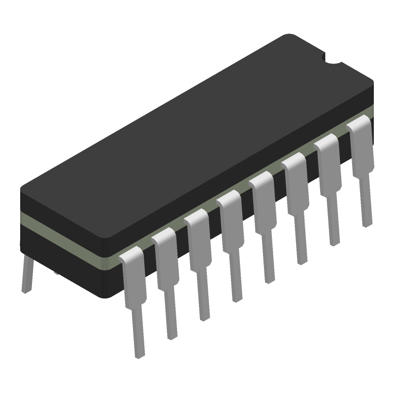
3D Model
Available Download Formats
By downloading CAD models, you agree to our Terms & Conditions and Privacy Policy

CMOS Quad NAND R/S Latch with 3-State Outputs 16-CDIP -55 to 125
Tip: Data for a part may vary between manufacturers. You can filter for manufacturers on the top of the page next to the part image and part number.
CD4044BF3A by Texas Instruments is an FF/Latch.
FF/Latches are under the broader part category of Logic Components.
Digital logic governs the behavior of signals in electronic circuits, enabling complex decisions based on simple binary inputs (yes/no). Logic components perform operations from these signals. Read more about Logic Components on our Logic part category page.
| Part # | Manufacturer | Description | Datasheet |
|---|---|---|---|
| CD4044BF3A | Texas Instruments | CMOS Quad NAND R/S Latch with 3-State Outputs 16-CDIP -55 to 125 |
| Part # | Distributor | Description | Stock | Price | Buy | |
|---|---|---|---|---|---|---|
|
DISTI #
296-CD4044BF3A-ND
|
DigiKey | CMOS QUAD NAND R/S LATCH WITH 3- Lead time: 12 Weeks Container: Tube | Temporarily Out of Stock |
|
Buy Now | |
|
DISTI #
J56:1989_00547891
|
Arrow Electronics | Latch Transparent 3-ST 4-CH SR-Type 16-Pin CDIP Tube RoHS: Not Compliant Min Qty: 1 Package Multiple: 1 Lead time: 12 Weeks | Europe - 44 |
|
$12.5700 | Buy Now |
|
|
Bristol Electronics | 19 |
|
RFQ | ||
|
|
Quest Components | 4000/14000/40000 SERIES, LOW LEVEL TRIGGERED R-S LATCH, TRUE OUTPUT, CDIP16 | 20 |
|
$12.3106 / $14.9724 | Buy Now |
|
|
Quest Components | 4000/14000/40000 SERIES, LOW LEVEL TRIGGERED R-S LATCH, TRUE OUTPUT, CDIP16 | 15 |
|
$16.1921 / $19.6931 | Buy Now |
By downloading CAD models, you agree to our Terms & Conditions and Privacy Policy
|
|
CD4044BF3A
Texas Instruments
Buy Now
Datasheet
|
Compare Parts:
CD4044BF3A
Texas Instruments
CMOS Quad NAND R/S Latch with 3-State Outputs 16-CDIP -55 to 125
|
| Pbfree Code | Yes | |
| Rohs Code | No | |
| Part Life Cycle Code | Active | |
| Ihs Manufacturer | TEXAS INSTRUMENTS INC | |
| Part Package Code | DIP | |
| Pin Count | 16 | |
| Reach Compliance Code | not_compliant | |
| ECCN Code | EAR99 | |
| HTS Code | 8542.39.00.01 | |
| Samacsys Manufacturer | Texas Instruments | |
| Family | 4000/14000/40000 | |
| JESD-30 Code | R-GDIP-T16 | |
| JESD-609 Code | e0 | |
| Length | 19.56 mm | |
| Load Capacitance (CL) | 50 pF | |
| Logic IC Type | R-S LATCH | |
| Max I(ol) | 0.0024 A | |
| Number of Bits | 4 | |
| Number of Functions | 4 | |
| Number of Terminals | 16 | |
| Operating Temperature-Max | 125 °C | |
| Operating Temperature-Min | -55 °C | |
| Output Characteristics | 3-STATE | |
| Output Polarity | TRUE | |
| Package Body Material | CERAMIC, GLASS-SEALED | |
| Package Code | DIP | |
| Package Equivalence Code | DIP16,.3 | |
| Package Shape | RECTANGULAR | |
| Package Style | IN-LINE | |
| Packing Method | TUBE | |
| Power Supply Current-Max (ICC) | 0.06 mA | |
| Prop. Delay@Nom-Sup | 140 ns | |
| Propagation Delay (tpd) | 300 ns | |
| Qualification Status | Not Qualified | |
| Schmitt Trigger | NO | |
| Screening Level | 38535Q/M;38534H;883B | |
| Seated Height-Max | 5.08 mm | |
| Supply Voltage-Max (Vsup) | 18 V | |
| Supply Voltage-Min (Vsup) | 3 V | |
| Supply Voltage-Nom (Vsup) | 5 V | |
| Surface Mount | NO | |
| Technology | CMOS | |
| Temperature Grade | MILITARY | |
| Terminal Finish | Tin/Lead (Sn/Pb) | |
| Terminal Form | THROUGH-HOLE | |
| Terminal Pitch | 2.54 mm | |
| Terminal Position | DUAL | |
| Trigger Type | LOW LEVEL | |
| Width | 7.62 mm |
This table gives cross-reference parts and alternative options found for CD4044BF3A. The Form Fit Function (FFF) tab will give you the options that are more likely to serve as direct pin-to-pin alternates or drop-in parts. The Functional Equivalents tab will give you options that are likely to match the same function of CD4044BF3A, but it may not fit your design. Always verify details of parts you are evaluating, as these parts are offered as suggestions for what you are looking for and are not guaranteed.
| Part Number | Manufacturer | Composite Price | Description | Compare |
|---|---|---|---|---|
| CD4044BD3 | Harris Semiconductor | Check for Price | R-S Latch, 4000/14000/40000 Series, 1-Func, Low Level Triggered, 4-Bit, True Output, CMOS, CDIP16, METAL SEALED, CERAMIC, DIP-16 | CD4044BF3A vs CD4044BD3 |
The recommended operating voltage range for CD4044BF3A is 4.5V to 15V, although the datasheet specifies a minimum of 3V. Operating outside this range may affect the device's performance and reliability.
To ensure proper power sequencing, it's recommended to power up the CD4044BF3A after the power supply has stabilized. You can use a power-on reset circuit or a voltage supervisor to ensure the device is powered up correctly.
The maximum clock frequency that CD4044BF3A can handle is approximately 10 MHz. However, this may vary depending on the specific application and operating conditions.
The output enable (OE) pin is active-low, meaning it should be connected to GND to enable the outputs. When OE is high, the outputs are in a high-impedance state. Make sure to connect OE to a valid logic level to avoid output contention.
The VCC pin is the power supply pin for the internal logic of the CD4044BF3A. It should be connected to a stable power supply voltage between 4.5V and 15V.