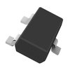
Part Details for BSS138BKW by NXP Semiconductors
Results Overview of BSS138BKW by NXP Semiconductors
- Distributor Offerings: (3 listings)
- Number of FFF Equivalents: (0 replacements)
- CAD Models: (Request Part)
- Number of Functional Equivalents: (1 option)
- Part Data Attributes: (Available)
- Reference Designs: (Not Available)
Tip: Data for a part may vary between manufacturers. You can filter for manufacturers on the top of the page next to the part image and part number.
BSS138BKW Information
BSS138BKW by NXP Semiconductors is a Small Signal Field-Effect Transistor.
Small Signal Field-Effect Transistors are under the broader part category of Transistors.
A transistor is a small semiconductor device used to amplify, control, or create electrical signals. When selecting a transistor, factors such as voltage, current rating, gain, and power dissipation must be considered, with common types. Read more about Transistors on our Transistors part category page.
Price & Stock for BSS138BKW
| Part # | Distributor | Description | Stock | Price | Buy | |
|---|---|---|---|---|---|---|
|
|
ComSIT USA | 60 V, 320 MILLI AMP N-CHANNEL TRENCH MOSFET Small Signal Field-Effect Transistor, 0.32A I(D), 60V, 1-Element, N-Channel, Silicon, Metal-oxide Semiconductor FET ECCN: EAR99 RoHS: Compliant |
|
|
RFQ | |
|
|
Vyrian | Transistors | 16550 |
|
RFQ | |
|
|
Win Source Electronics | 60 V, 320 mA N-channel Trench MOSFET | 120000 |
|
$0.0289 / $0.0372 | Buy Now |
Part Details for BSS138BKW
BSS138BKW CAD Models
BSS138BKW Part Data Attributes
|
|
BSS138BKW
NXP Semiconductors
Buy Now
Datasheet
|
Compare Parts:
BSS138BKW
NXP Semiconductors
320mA, 60V, N-CHANNEL, Si, SMALL SIGNAL, MOSFET, PLASTIC, SC-70, 3 PIN
|
| Rohs Code | Yes | |
| Part Life Cycle Code | Transferred | |
| Ihs Manufacturer | NXP SEMICONDUCTORS | |
| Part Package Code | SC-70 | |
| Package Description | PLASTIC, SC-70, 3 PIN | |
| Pin Count | 3 | |
| Reach Compliance Code | unknown | |
| ECCN Code | EAR99 | |
| Samacsys Manufacturer | NXP | |
| Additional Feature | LOGIC LEVEL COMPATIBLE | |
| Configuration | SINGLE WITH BUILT-IN DIODE | |
| DS Breakdown Voltage-Min | 60 V | |
| Drain Current-Max (ID) | 0.32 A | |
| Drain-source On Resistance-Max | 1.6 Ω | |
| FET Technology | METAL-OXIDE SEMICONDUCTOR | |
| JESD-30 Code | R-PDSO-G3 | |
| JESD-609 Code | e3 | |
| Moisture Sensitivity Level | 1 | |
| Number of Elements | 1 | |
| Number of Terminals | 3 | |
| Operating Mode | ENHANCEMENT MODE | |
| Package Body Material | PLASTIC/EPOXY | |
| Package Shape | RECTANGULAR | |
| Package Style | SMALL OUTLINE | |
| Peak Reflow Temperature (Cel) | NOT SPECIFIED | |
| Polarity/Channel Type | N-CHANNEL | |
| Surface Mount | YES | |
| Terminal Finish | Tin (Sn) | |
| Terminal Form | GULL WING | |
| Terminal Position | DUAL | |
| Time@Peak Reflow Temperature-Max (s) | NOT SPECIFIED | |
| Transistor Application | SWITCHING | |
| Transistor Element Material | SILICON |
Alternate Parts for BSS138BKW
This table gives cross-reference parts and alternative options found for BSS138BKW. The Form Fit Function (FFF) tab will give you the options that are more likely to serve as direct pin-to-pin alternates or drop-in parts. The Functional Equivalents tab will give you options that are likely to match the same function of BSS138BKW, but it may not fit your design. Always verify details of parts you are evaluating, as these parts are offered as suggestions for what you are looking for and are not guaranteed.
| Part Number | Manufacturer | Composite Price | Description | Compare |
|---|---|---|---|---|
| BSS138BKW,115 | NXP Semiconductors | Check for Price | BSS138BKW - 60 V, 320 mA N-channel Trench MOSFET SC-70 3-Pin | BSS138BKW vs BSS138BKW,115 |
BSS138BKW Frequently Asked Questions (FAQ)
-
The maximum operating temperature range for the BSS138BKW is -55°C to 150°C, as specified in the datasheet. However, it's recommended to operate the device within a temperature range of -40°C to 125°C for optimal performance and reliability.
-
To ensure proper biasing, make sure to provide a stable voltage supply to the gate-source voltage (VGS) within the recommended range of 1.5V to 5V. Additionally, ensure the drain-source voltage (VDS) is within the recommended range of 0V to 50V. Proper biasing is critical for optimal performance, low power consumption, and high reliability.
-
For optimal thermal management, it's recommended to use a PCB layout with a large copper area connected to the drain pin to dissipate heat efficiently. Additionally, ensure good thermal conductivity between the device and the PCB by using a thermal interface material (TIM) or a thermal pad. A well-designed PCB layout and thermal management can help reduce thermal resistance and improve overall device performance.
-
To protect the BSS138BKW from ESD, handle the device with care, and use ESD-safe equipment and materials during assembly and testing. Ensure the device is stored in an ESD-safe environment, and use ESD protection devices such as TVS diodes or ESD protection arrays in the circuit design. Additionally, follow proper ESD handling procedures, such as grounding yourself before handling the device.
-
For optimal soldering, follow the recommended soldering conditions specified in the datasheet. The recommended soldering temperature is 260°C (peak temperature) with a soldering time of 10 seconds (max). Ensure the soldering process is done in a controlled environment with minimal thermal stress to prevent damage to the device.
