-
Part Symbol
-
Footprint
-
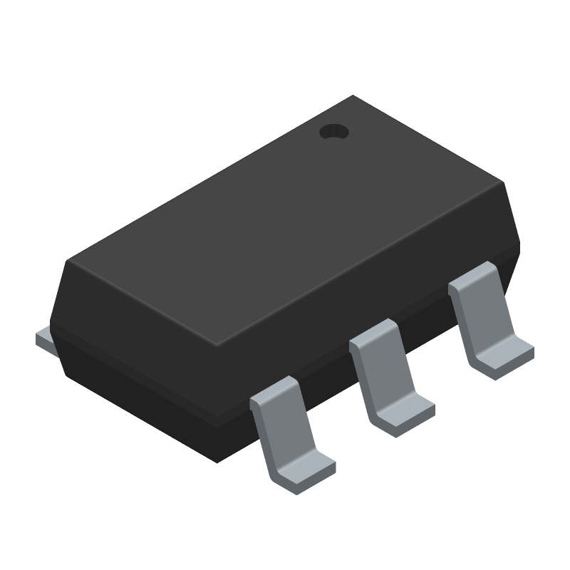
3D Model
Available Download Formats
By downloading CAD models, you agree to our Terms & Conditions and Privacy Policy

Power Field-Effect Transistor, 6.3A I(D), 30V, 0.033ohm, 1-Element, P-Channel, Silicon, Metal-oxide Semiconductor FET, TSOP-6
Tip: Data for a part may vary between manufacturers. You can filter for manufacturers on the top of the page next to the part image and part number.
BSL303SPEH6327XTSA1 by Infineon Technologies AG is a Power Field-Effect Transistor.
Power Field-Effect Transistors are under the broader part category of Transistors.
A transistor is a small semiconductor device used to amplify, control, or create electrical signals. When selecting a transistor, factors such as voltage, current rating, gain, and power dissipation must be considered, with common types. Read more about Transistors on our Transistors part category page.
| Part # | Distributor | Description | Stock | Price | Buy | |
|---|---|---|---|---|---|---|
|
DISTI #
SP000953144
|
EBV Elektronik | Trans MOSFET PCH 30V 63A 6pin TSOP TR (Alt: SP000953144) RoHS: Compliant Min Qty: 3000 Package Multiple: 3000 Lead time: 143 Weeks, 0 Days | EBV - 0 |
|
Buy Now |
By downloading CAD models, you agree to our Terms & Conditions and Privacy Policy
|
|
BSL303SPEH6327XTSA1
Infineon Technologies AG
Buy Now
Datasheet
|
Compare Parts:
BSL303SPEH6327XTSA1
Infineon Technologies AG
Power Field-Effect Transistor, 6.3A I(D), 30V, 0.033ohm, 1-Element, P-Channel, Silicon, Metal-oxide Semiconductor FET, TSOP-6
|
| Pbfree Code | Yes | |
| Rohs Code | Yes | |
| Part Life Cycle Code | Obsolete | |
| Ihs Manufacturer | INFINEON TECHNOLOGIES AG | |
| Package Description | TSOP-6 | |
| Reach Compliance Code | compliant | |
| ECCN Code | EAR99 | |
| Samacsys Manufacturer | Infineon | |
| Additional Feature | AVALANCHE RATED | |
| Avalanche Energy Rating (Eas) | 30 mJ | |
| Configuration | SINGLE WITH BUILT-IN DIODE | |
| DS Breakdown Voltage-Min | 30 V | |
| Drain Current-Max (ID) | 6.3 A | |
| Drain-source On Resistance-Max | 0.033 Ω | |
| FET Technology | METAL-OXIDE SEMICONDUCTOR | |
| JESD-30 Code | R-PDSO-G6 | |
| JESD-609 Code | e3 | |
| Number of Elements | 1 | |
| Number of Terminals | 6 | |
| Operating Mode | ENHANCEMENT MODE | |
| Package Body Material | PLASTIC/EPOXY | |
| Package Shape | RECTANGULAR | |
| Package Style | SMALL OUTLINE | |
| Polarity/Channel Type | P-CHANNEL | |
| Pulsed Drain Current-Max (IDM) | 25.2 A | |
| Reference Standard | AEC-Q101 | |
| Surface Mount | YES | |
| Terminal Finish | TIN | |
| Terminal Form | GULL WING | |
| Terminal Position | DUAL | |
| Transistor Element Material | SILICON |
The recommended PCB layout for optimal thermal performance involves using a 2-layer or 4-layer board with a solid ground plane, and placing thermal vias under the device to dissipate heat efficiently.
To ensure EMC, use a shielded enclosure, keep the device away from high-frequency sources, and use a common-mode choke or ferrite bead to filter out electromagnetic interference.
The maximum allowed voltage transient on the input pins is 20% above the maximum recommended operating voltage, but it's recommended to use a TVS diode or a voltage clamp to protect the device from voltage spikes.
While the device is rated for operation up to 150°C, it's recommended to derate the current and voltage at higher temperatures to ensure reliable operation and prevent thermal runaway.
Check the input voltage, output voltage, and current sense resistors for correct values and connections. Verify that the enable pin is properly biased, and check for any signs of overheating or physical damage.