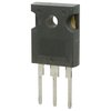
Part Details for APT34F100B2 by Microsemi Corporation
Results Overview of APT34F100B2 by Microsemi Corporation
- Distributor Offerings: (1 listing)
- Number of FFF Equivalents: (0 replacements)
- CAD Models: (Request Part)
- Number of Functional Equivalents: (0 options)
- Part Data Attributes: (Available)
- Reference Designs: (Not Available)
Tip: Data for a part may vary between manufacturers. You can filter for manufacturers on the top of the page next to the part image and part number.
APT34F100B2 Information
APT34F100B2 by Microsemi Corporation is a Power Field-Effect Transistor.
Power Field-Effect Transistors are under the broader part category of Transistors.
A transistor is a small semiconductor device used to amplify, control, or create electrical signals. When selecting a transistor, factors such as voltage, current rating, gain, and power dissipation must be considered, with common types. Read more about Transistors on our Transistors part category page.
Price & Stock for APT34F100B2
| Part # | Distributor | Description | Stock | Price | Buy | |
|---|---|---|---|---|---|---|
|
DISTI #
34833790
|
Verical | Trans MOSFET N-CH Si 1KV 35A 3-Pin(3+Tab) T-MAX Tube RoHS: Compliant Min Qty: 3 Package Multiple: 1 Date Code: 1932 | Americas - 13 |
|
$25.4500 | Buy Now |
Part Details for APT34F100B2
APT34F100B2 CAD Models
APT34F100B2 Part Data Attributes
|
|
APT34F100B2
Microsemi Corporation
Buy Now
Datasheet
|
Compare Parts:
APT34F100B2
Microsemi Corporation
Power Field-Effect Transistor, 35A I(D), 1000V, 0.38ohm, 1-Element, N-Channel, Silicon, Metal-oxide Semiconductor FET, TO-247AB, ROHS COMPLIANT, T-MAX, 3 PIN
|
| Pbfree Code | Yes | |
| Rohs Code | Yes | |
| Part Life Cycle Code | Transferred | |
| Ihs Manufacturer | MICROSEMI CORP | |
| Part Package Code | TO-247AB | |
| Package Description | ROHS COMPLIANT, T-MAX, 3 PIN | |
| Pin Count | 3 | |
| Reach Compliance Code | unknown | |
| ECCN Code | EAR99 | |
| Additional Feature | AVALANCHE RATED, HIGH RELIABILITY | |
| Avalanche Energy Rating (Eas) | 2165 mJ | |
| Case Connection | DRAIN | |
| Configuration | SINGLE WITH BUILT-IN DIODE | |
| DS Breakdown Voltage-Min | 1000 V | |
| Drain Current-Max (ID) | 35 A | |
| Drain-source On Resistance-Max | 0.38 Ω | |
| FET Technology | METAL-OXIDE SEMICONDUCTOR | |
| JEDEC-95 Code | TO-247AB | |
| JESD-30 Code | R-PSIP-T3 | |
| Number of Elements | 1 | |
| Number of Terminals | 3 | |
| Operating Mode | ENHANCEMENT MODE | |
| Operating Temperature-Max | 150 °C | |
| Package Body Material | PLASTIC/EPOXY | |
| Package Shape | RECTANGULAR | |
| Package Style | IN-LINE | |
| Polarity/Channel Type | N-CHANNEL | |
| Pulsed Drain Current-Max (IDM) | 140 A | |
| Qualification Status | Not Qualified | |
| Surface Mount | NO | |
| Terminal Finish | PURE MATTE TIN | |
| Terminal Form | THROUGH-HOLE | |
| Terminal Position | SINGLE | |
| Transistor Application | SWITCHING | |
| Transistor Element Material | SILICON |
APT34F100B2 Frequently Asked Questions (FAQ)
-
Microsemi recommends following the guidelines in the 'APT34F100B2 PCB Layout and Thermal Management Application Note' (document number 13034) for optimal performance and thermal management. This includes using a 4-layer PCB with a solid ground plane, placing thermal vias under the device, and using a heat sink with a thermal interface material.
-
To ensure reliable operation in high-temperature environments, it's essential to follow the recommended operating conditions and derating guidelines in the datasheet. Additionally, consider using a heat sink, thermal interface material, and ensuring good airflow around the device. Microsemi also recommends using a thermocouple to monitor the device temperature and implementing thermal shutdown or warning mechanisms in the system design.
-
The APT34F100B2 has built-in ESD protection, but it's still essential to follow proper ESD handling and storage procedures to prevent damage. Microsemi recommends using an ESD wrist strap, mat, or workstation, and storing the devices in anti-static packaging. The device should be handled by the body only, and not by the leads, to prevent damage.
-
The APT34F100B2 is not specifically designed or qualified for radiation-hardened or high-reliability applications. However, Microsemi offers other products that are designed and tested for these types of applications. Engineers should contact Microsemi directly to discuss their specific requirements and determine the most suitable device for their application.
-
Microsemi recommends following the guidelines in the 'APT34F100B2 Soldering and Rework Application Note' (document number 13035) for soldering and rework procedures. This includes using a soldering iron with a temperature range of 250°C to 260°C, and a solder with a melting point above 217°C. The device should be soldered within 10 seconds, and rework should be performed within 3 attempts.
