-
Part Symbol
-
Footprint
-
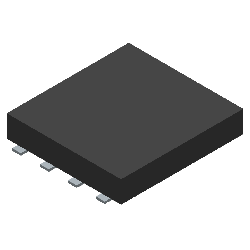
3D Model
Available Download Formats
By downloading CAD models, you agree to our Terms & Conditions and Privacy Policy
Transistor
Tip: Data for a part may vary between manufacturers. You can filter for manufacturers on the top of the page next to the part image and part number.
AON6816 by Alpha & Omega Semiconductor is an Other Transistor.
Other Transistors are under the broader part category of Transistors.
A transistor is a small semiconductor device used to amplify, control, or create electrical signals. When selecting a transistor, factors such as voltage, current rating, gain, and power dissipation must be considered, with common types. Read more about Transistors on our Transistors part category page.
| Part # | Distributor | Description | Stock | Price | Buy | |
|---|---|---|---|---|---|---|
|
DISTI #
785-1499-1-ND
|
DigiKey | MOSFET 2N-CH 30V 17A 8DFN Min Qty: 1 Lead time: 16 Weeks Container: Digi-Reel®, Cut Tape (CT), Tape & Reel (TR) |
21734 In Stock |
|
$0.3650 / $1.5400 | Buy Now |
|
DISTI #
AON6816
|
TME | Transistor: N-MOSFET x2, unipolar, 30V, 13A, 8W, DFN5x6B Min Qty: 1 | 0 |
|
$0.3280 / $0.7180 | RFQ |
By downloading CAD models, you agree to our Terms & Conditions and Privacy Policy
|
|
AON6816
Alpha & Omega Semiconductor
Buy Now
Datasheet
|
Compare Parts:
AON6816
Alpha & Omega Semiconductor
Transistor
|
| Rohs Code | Yes | |
| Part Life Cycle Code | Active | |
| Ihs Manufacturer | ALPHA & OMEGA SEMICONDUCTOR LTD | |
| Reach Compliance Code | compliant | |
| ECCN Code | EAR99 | |
| Samacsys Manufacturer | Alpha & Omega Semiconductors |
The AON6816 can operate from -55°C to 150°C, making it suitable for high-reliability applications.
To ensure proper biasing, connect the gate to a voltage source through a resistor, and connect the source to ground through a resistor. The recommended bias voltage is 10V to 15V.
The AON6816 has a maximum continuous drain current rating of 30A, and a maximum pulsed drain current rating of 60A.
To protect the AON6816 from ESD, handle the device with an anti-static wrist strap or mat, and ensure that all equipment is properly grounded. Avoid touching the device's pins or leads.
To minimize thermal resistance and ensure optimal performance, use a multi-layer PCB with a thermal pad connected to a heat sink or a large copper area. Keep the drain and source pins as close as possible to reduce inductance.