-
Part Symbol
-
Footprint
-
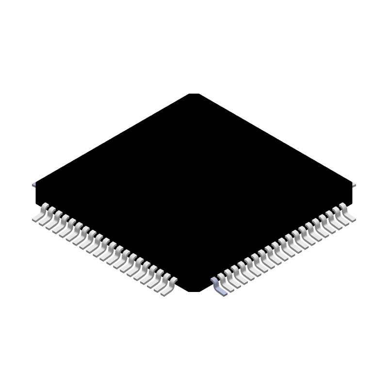
3D Model
Available Download Formats
By downloading CAD models, you agree to our Terms & Conditions and Privacy Policy

13-bit 250-MSPS analog-to-digital converter (ADC) - enhanced product 80-HTQFP -55 to 125
Tip: Data for a part may vary between manufacturers. You can filter for manufacturers on the top of the page next to the part image and part number.
ADS5444MPFPEP by Texas Instruments is an Analog to Digital Converter.
Analog to Digital Converters are under the broader part category of Converters.
A converter is an electrical circuit that transforms electric energy into a different form that will support a elecrical load needed by a device. Read more about Converters on our Converters part category page.
| Part # | Manufacturer | Description | Datasheet |
|---|---|---|---|
| ADS5444MPFPEP | Texas Instruments | 13-Bit, 250-MSPS Analog-to-Digital Converter (ADC) - Enhanced-Product 80-HTQFP -55 to 125 |
| Part # | Distributor | Description | Stock | Price | Buy | |
|---|---|---|---|---|---|---|
|
DISTI #
296-20673-ND
|
DigiKey | IC ADC 13BIT PIPELINED 80HTQFP Min Qty: 1 Lead time: 18 Weeks Container: Tray | Temporarily Out of Stock |
|
$175.6000 / $214.6100 | Buy Now |
|
DISTI #
595-ADS5444MPFPEP
|
Mouser Electronics | Analog to Digital Converters - ADC EP 13B 250MSPS ADC RoHS: Compliant | 0 |
|
$174.0000 | Order Now |
By downloading CAD models, you agree to our Terms & Conditions and Privacy Policy
|
|
ADS5444MPFPEP
Texas Instruments
Buy Now
Datasheet
|
Compare Parts:
ADS5444MPFPEP
Texas Instruments
13-bit 250-MSPS analog-to-digital converter (ADC) - enhanced product 80-HTQFP -55 to 125
|
| Pbfree Code | Yes | |
| Rohs Code | Yes | |
| Part Life Cycle Code | Active | |
| Ihs Manufacturer | TEXAS INSTRUMENTS INC | |
| Part Package Code | QFP | |
| Package Description | HTFQFP, TQFP80,.55SQ | |
| Pin Count | 80 | |
| Reach Compliance Code | compliant | |
| ECCN Code | 3A001.A.2.C | |
| HTS Code | 8542.39.00.01 | |
| Samacsys Manufacturer | Texas Instruments | |
| Additional Feature | Peak-to-peak input voltage range(V) : 2.2 | |
| Analog Input Voltage-Max | 2.2 V | |
| Analog Input Voltage-Min | -2.2 V | |
| Converter Type | ADC, PROPRIETARY METHOD | |
| JESD-30 Code | S-PQFP-G80 | |
| JESD-609 Code | e4 | |
| Length | 12 mm | |
| Linearity Error-Max (EL) | 0.0525% | |
| Moisture Sensitivity Level | 3 | |
| Number of Analog In Channels | 1 | |
| Number of Bits | 13 | |
| Number of Functions | 1 | |
| Number of Terminals | 80 | |
| Operating Temperature-Max | 125 °C | |
| Operating Temperature-Min | -55 °C | |
| Output Bit Code | OFFSET BINARY | |
| Output Format | PARALLEL, WORD | |
| Package Body Material | PLASTIC/EPOXY | |
| Package Code | HTFQFP | |
| Package Equivalence Code | TQFP80,.55SQ | |
| Package Shape | SQUARE | |
| Package Style | FLATPACK, HEAT SINK/SLUG, THIN PROFILE, FINE PITCH | |
| Peak Reflow Temperature (Cel) | 260 | |
| Qualification Status | Not Qualified | |
| Sample Rate | 250 MHz | |
| Sample and Hold / Track and Hold | TRACK | |
| Seated Height-Max | 1.2 mm | |
| Supply Current-Max | 430 mA | |
| Supply Voltage-Nom | 5 V | |
| Surface Mount | YES | |
| Technology | BIPOLAR | |
| Temperature Grade | MILITARY | |
| Terminal Finish | Nickel/Palladium/Gold (Ni/Pd/Au) | |
| Terminal Form | GULL WING | |
| Terminal Pitch | 0.5 mm | |
| Terminal Position | QUAD | |
| Time@Peak Reflow Temperature-Max (s) | 30 | |
| Width | 12 mm |
The recommended power-up sequence is to apply the analog power supply (AVDD) first, followed by the digital power supply (DVDD), and then the clock signal. This ensures proper initialization of the device.
To optimize the analog input impedance, use a low-impedance source, such as a buffer amplifier, and ensure that the input signal is properly terminated. Additionally, consider using a differential input configuration to reduce common-mode noise.
The ADS5444MPFPEP supports clock frequencies up to 160 MSPS. However, the maximum clock frequency may vary depending on the specific application and system requirements.
Metastability issues can be handled by using a synchronizer circuit or a metastable-resistant flip-flop to resynchronize the data output. Additionally, consider using a clock domain crossing (CDC) circuit to ensure proper data transfer between clock domains.
To minimize noise and ensure proper operation, follow a star-grounding scheme, keep analog and digital signals separate, and use a solid ground plane. Additionally, consider using a 4-layer PCB with a dedicated power plane and a dedicated ground plane.