-
Part Symbol
-
Footprint
-
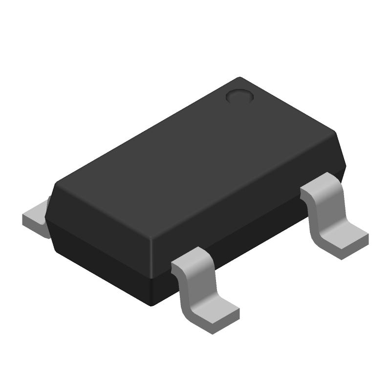
3D Model
Available Download Formats
By downloading CAD models, you agree to our Terms & Conditions and Privacy Policy
40 V, 200 mA, Low Noise, CMOS LDO Linear Regulator
Tip: Data for a part may vary between manufacturers. You can filter for manufacturers on the top of the page next to the part image and part number.
ADP7142AUJZ-R2 by Analog Devices Inc is a Linear Regulator IC.
Linear Regulator ICs are under the broader part category of Power Circuits.
A power circuit delivers electricity in order to operate a load for an electronic device. Power circuits include transformers, generators and switches. Read more about Power Circuits on our Power Circuits part category page.
| Part # | Distributor | Description | Stock | Price | Buy | |
|---|---|---|---|---|---|---|
|
|
Analog Devices Inc | 40V 200mA LDO adjVo Min Qty: 250 Package Multiple: 250 | 13500 |
|
$1.5200 | Buy Now |
|
|
Vyrian | Regulators | 16243 |
|
RFQ |
By downloading CAD models, you agree to our Terms & Conditions and Privacy Policy
|
|
ADP7142AUJZ-R2
Analog Devices Inc
Buy Now
Datasheet
|
Compare Parts:
ADP7142AUJZ-R2
Analog Devices Inc
40 V, 200 mA, Low Noise, CMOS LDO Linear Regulator
|
| Pbfree Code | No | |
| Rohs Code | Yes | |
| Part Life Cycle Code | Active | |
| Ihs Manufacturer | ANALOG DEVICES INC | |
| Pin Count | 5 | |
| Manufacturer Package Code | UJ-5 | |
| Reach Compliance Code | compliant | |
| ECCN Code | EAR99 | |
| HTS Code | 8542.39.00.01 | |
| Samacsys Manufacturer | Analog Devices | |
| Dropout Voltage1-Max | 0.42 V | |
| JESD-30 Code | R-PDSO-G5 | |
| JESD-609 Code | e3 | |
| Length | 2.9 mm | |
| Moisture Sensitivity Level | 1 | |
| Number of Functions | 1 | |
| Number of Terminals | 5 | |
| Operating Temperature TJ-Max | 125 °C | |
| Operating Temperature TJ-Min | -40 °C | |
| Output Current1-Max | 0.2 A | |
| Output Voltage1-Max | 39.58 V | |
| Output Voltage1-Min | 1.2 V | |
| Package Body Material | PLASTIC/EPOXY | |
| Package Code | VSSOP | |
| Package Shape | RECTANGULAR | |
| Package Style | SMALL OUTLINE, VERY THIN PROFILE, SHRINK PITCH | |
| Peak Reflow Temperature (Cel) | 260 | |
| Regulator Type | ADJUSTABLE POSITIVE SINGLE OUTPUT LDO REGULATOR | |
| Seated Height-Max | 1 mm | |
| Surface Mount | YES | |
| Technology | CMOS | |
| Terminal Finish | Matte Tin (Sn) | |
| Terminal Form | GULL WING | |
| Terminal Pitch | 0.95 mm | |
| Terminal Position | DUAL | |
| Time@Peak Reflow Temperature-Max (s) | 30 | |
| Width | 1.6 mm |
A good PCB layout for the ADP7142AUJZ-R2 involves keeping the input and output traces separate, using a solid ground plane, and placing the input and output capacitors close to the device. Additionally, it's recommended to use a 4-layer PCB with a dedicated power plane and a dedicated ground plane to minimize noise and EMI.
To ensure stability, it's essential to follow the recommended compensation network and component values provided in the datasheet. Additionally, the output capacitor should be selected based on the output voltage and current requirements, and the input capacitor should be chosen to filter out high-frequency noise. Proper PCB layout and decoupling are also crucial for stability.
The ADP7142AUJZ-R2 has an absolute maximum input voltage rating of 12V. However, the recommended input voltage range is 2.7V to 5.5V. Exceeding the absolute maximum rating can damage the device.
The ADP7142AUJZ-R2 is rated for operation from -40°C to 125°C. However, the device's performance and reliability may degrade at high temperatures. It's essential to follow the recommended operating conditions and derate the device's performance accordingly.
The output voltage of the ADP7142AUJZ-R2 can be calculated using the formula: VOUT = VREF x (1 + R1/R2), where VREF is the internal reference voltage (1.25V), R1 is the feedback resistor, and R2 is the divider resistor. The output voltage range is 0.8V to 5.5V.