-
Part Symbol
-
Footprint
-
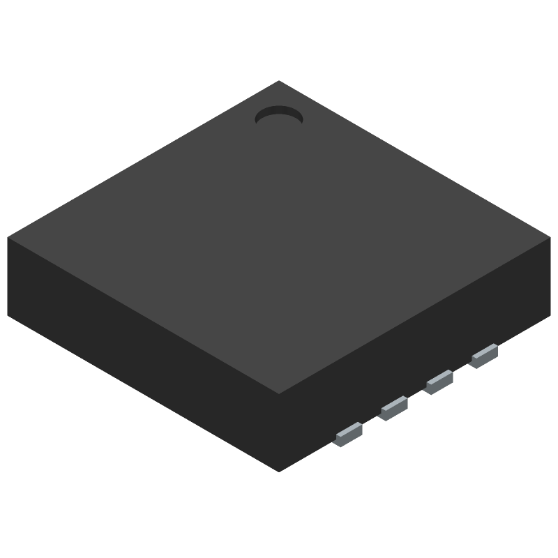
3D Model
Available Download Formats
By downloading CAD models, you agree to our Terms & Conditions and Privacy Policy

20 V, 300 mA, Low Noise, CMOS LDO
Tip: Data for a part may vary between manufacturers. You can filter for manufacturers on the top of the page next to the part image and part number.
ADP7102ACPZ-1.5-R7 by Analog Devices Inc is a Linear Regulator IC.
Linear Regulator ICs are under the broader part category of Power Circuits.
A power circuit delivers electricity in order to operate a load for an electronic device. Power circuits include transformers, generators and switches. Read more about Power Circuits on our Power Circuits part category page.
| Part # | Distributor | Description | Stock | Price | Buy | |
|---|---|---|---|---|---|---|
|
DISTI #
ADP7102ACPZ-1.5-R7CT-ND
|
DigiKey | IC REG LIN 1.5V 300MA 8-LFCSP-WD Min Qty: 1 Lead time: 10 Weeks Container: Digi-Reel®, Cut Tape (CT), Tape & Reel (TR) |
1286 In Stock |
|
$2.0750 / $5.5900 | Buy Now |
|
DISTI #
584-ADP7102ACPZ1.5R7
|
Mouser Electronics | Linear Voltage Regulators 300mA HV LDO 1.5V RoHS: Compliant | 1195 |
|
$2.0700 / $4.1400 | Buy Now |
|
|
Analog Devices Inc | 300mA HV LDO 1.5V Min Qty: 1 Package Multiple: 1500 | 258 |
|
$1.5700 / $5.5900 | Buy Now |
|
|
Quest Components | 279 |
|
$2.7876 / $4.5204 | Buy Now | |
|
|
Rochester Electronics | ADP7102 - 20V, 300mA, Low Noise, CMOS LDO RoHS: Compliant Status: Active Min Qty: 1 | 12961 |
|
$1.7400 / $2.1800 | Buy Now |
By downloading CAD models, you agree to our Terms & Conditions and Privacy Policy
|
|
ADP7102ACPZ-1.5-R7
Analog Devices Inc
Buy Now
Datasheet
|
Compare Parts:
ADP7102ACPZ-1.5-R7
Analog Devices Inc
20 V, 300 mA, Low Noise, CMOS LDO
|
| Pbfree Code | No | |
| Rohs Code | Yes | |
| Part Life Cycle Code | Active | |
| Ihs Manufacturer | ANALOG DEVICES INC | |
| Part Package Code | SON | |
| Package Description | 3 X 3 MM, ROHS COMPLIANT, MO-229WEED-4, LFCSP-8 | |
| Pin Count | 8 | |
| Manufacturer Package Code | CP-8-5 | |
| Reach Compliance Code | compliant | |
| ECCN Code | EAR99 | |
| HTS Code | 8542.39.00.01 | |
| Samacsys Manufacturer | Analog Devices | |
| Dropout Voltage1-Max | 1 V | |
| Dropout Voltage1-Nom | 1 V | |
| Input Voltage-Max | 20 V | |
| Input Voltage-Min | 3.3 V | |
| JESD-30 Code | S-PDSO-N8 | |
| JESD-609 Code | e3 | |
| Length | 3 mm | |
| Load Regulation-Max | 0.004485% | |
| Moisture Sensitivity Level | 3 | |
| Number of Functions | 1 | |
| Number of Terminals | 8 | |
| Operating Temperature TJ-Max | 125 °C | |
| Operating Temperature TJ-Min | -40 °C | |
| Output Current1-Max | 0.3 A | |
| Output Voltage1-Max | 1.515 V | |
| Output Voltage1-Min | 1.47 V | |
| Output Voltage1-Nom | 1.5 V | |
| Package Body Material | PLASTIC/EPOXY | |
| Package Code | HVSON | |
| Package Shape | SQUARE | |
| Package Style | SMALL OUTLINE, HEAT SINK/SLUG, VERY THIN PROFILE | |
| Regulator Type | FIXED POSITIVE SINGLE OUTPUT LDO REGULATOR | |
| Seated Height-Max | 0.8 mm | |
| Surface Mount | YES | |
| Technology | CMOS | |
| Terminal Finish | Matte Tin (Sn) | |
| Terminal Form | NO LEAD | |
| Terminal Pitch | 0.5 mm | |
| Terminal Position | DUAL | |
| Voltage Tolerance-Max | 2% | |
| Width | 3 mm |
A good PCB layout for the ADP7102 involves keeping the input and output traces short and separate, using a solid ground plane, and placing the input and output capacitors close to the device. A 4-layer PCB with a dedicated power plane and a solid ground plane is recommended.
To ensure stability, it's essential to follow the recommended PCB layout, use the correct output capacitor value and type, and ensure that the input voltage is within the specified range. Additionally, adding a small capacitor (e.g., 10nF) between the VIN pin and GND can help prevent oscillations.
The ADP7102 is rated for operation up to 125°C ambient temperature, but it's recommended to derate the output current and voltage at higher temperatures to ensure reliable operation. Consult the datasheet for thermal derating curves.
Yes, the ADP7102 is qualified for automotive and high-reliability applications. It meets the AEC-Q100 standard for automotive grade and is manufactured using a high-reliability process. However, it's essential to follow the recommended design and layout guidelines to ensure reliable operation.
The power dissipation of the ADP7102 can be calculated using the formula: Pd = (VIN x IIN) + (VOUT x IOUT). Where VIN is the input voltage, IIN is the input current, VOUT is the output voltage, and IOUT is the output current. Consult the datasheet for thermal resistance values to calculate the junction temperature.