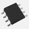
Part Details for ADP3603AR by Analog Devices Inc
Results Overview of ADP3603AR by Analog Devices Inc
- Distributor Offerings: (2 listings)
- Number of FFF Equivalents: (0 replacements)
- CAD Models: (Request Part)
- Number of Functional Equivalents: (0 options)
- Part Data Attributes: (Available)
- Reference Designs: (Not Available)
Tip: Data for a part may vary between manufacturers. You can filter for manufacturers on the top of the page next to the part image and part number.
ADP3603AR Information
ADP3603AR by Analog Devices Inc is a Switching Regulator or Controller.
Switching Regulator or Controllers are under the broader part category of Power Circuits.
A power circuit delivers electricity in order to operate a load for an electronic device. Power circuits include transformers, generators and switches. Read more about Power Circuits on our Power Circuits part category page.
Price & Stock for ADP3603AR
| Part # | Distributor | Description | Stock | Price | Buy | |
|---|---|---|---|---|---|---|
|
DISTI #
2156-ADP3603AR-ND
|
DigiKey | IC REG BUCK -3V 50MA 8SOIC Min Qty: 171 Lead time: 1 Weeks Container: Bulk MARKETPLACE PRODUCT |
42927 In Stock |
|
$1.7600 | Buy Now |
|
|
Rochester Electronics | Switched Capacitor Voltage Converter with Regulated Output RoHS: Not Compliant Status: Obsolete Min Qty: 1 | 42927 |
|
$1.3500 / $1.6900 | Buy Now |
Part Details for ADP3603AR
ADP3603AR CAD Models
ADP3603AR Part Data Attributes
|
|
ADP3603AR
Analog Devices Inc
Buy Now
Datasheet
|
Compare Parts:
ADP3603AR
Analog Devices Inc
IC SWITCHED CAPACITOR REGULATOR, 240 kHz SWITCHING FREQ-MAX, PDSO8, SOIC-8, Switching Regulator or Controller
|
| Rohs Code | No | |
| Part Life Cycle Code | Obsolete | |
| Ihs Manufacturer | ANALOG DEVICES INC | |
| Part Package Code | SOIC | |
| Package Description | SOIC-8 | |
| Pin Count | 8 | |
| Reach Compliance Code | not_compliant | |
| ECCN Code | EAR99 | |
| HTS Code | 8542.39.00.01 | |
| Analog IC - Other Type | SWITCHED CAPACITOR REGULATOR | |
| Control Mode | VOLTAGE-MODE | |
| Input Voltage-Max | 6 V | |
| Input Voltage-Min | 4.5 V | |
| Input Voltage-Nom | 5 V | |
| JESD-30 Code | R-PDSO-G8 | |
| JESD-609 Code | e0 | |
| Length | 4.9 mm | |
| Number of Functions | 1 | |
| Number of Terminals | 8 | |
| Operating Temperature-Max | 70 °C | |
| Operating Temperature-Min | ||
| Output Current-Max | 0.05 A | |
| Output Voltage-Nom | -3 V | |
| Package Body Material | PLASTIC/EPOXY | |
| Package Code | SOP | |
| Package Equivalence Code | SOP8,.25 | |
| Package Shape | RECTANGULAR | |
| Package Style | SMALL OUTLINE | |
| Qualification Status | Not Qualified | |
| Seated Height-Max | 1.75 mm | |
| Supply Current-Max (Isup) | 5 mA | |
| Surface Mount | YES | |
| Switcher Configuration | DOUBLER INVERTER | |
| Switching Frequency-Max | 240 kHz | |
| Technology | CMOS | |
| Temperature Grade | COMMERCIAL | |
| Terminal Finish | TIN LEAD | |
| Terminal Form | GULL WING | |
| Terminal Pitch | 1.27 mm | |
| Terminal Position | DUAL | |
| Width | 3.9 mm |
ADP3603AR Frequently Asked Questions (FAQ)
-
A good PCB layout is crucial for the ADP3603AR. Ensure a solid ground plane, keep the input and output traces short and separate, and use a common-mode choke to reduce EMI. Refer to the ADP3603AR evaluation board layout as a reference.
-
Choose X5R or X7R ceramic capacitors with a voltage rating of at least 2x the input voltage. For the input capacitor, select a value between 1uF to 10uF, and for the output capacitor, choose a value between 2.2uF to 22uF. Ensure the capacitors are placed close to the IC and have a low ESL.
-
The ADP3603AR can handle input voltages up to 36V, but it's recommended to operate within the specified range of 12V to 24V for optimal performance and reliability.
-
Ensure good thermal design and heat dissipation. Use a heat sink or a thermal pad, and keep the device away from heat sources. Monitor the junction temperature (TJ) and ensure it stays within the specified range of -40°C to 125°C.
-
To prevent damage, ensure the input voltage (VIN) is applied before the enable pin (EN) is asserted. When shutting down, assert the EN pin low before removing the input voltage.
