-
Part Symbol
-
Footprint
-
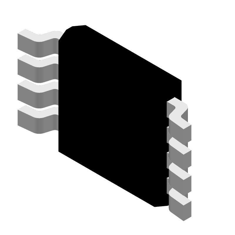
3D Model
Available Download Formats
By downloading CAD models, you agree to our Terms & Conditions and Privacy Policy

IC VREG 1.5 V FIXED POSITIVE LDO REGULATOR, 0.23 V DROPOUT, PDSO8, ROHS COMPLIANT, ULTRA SMALL, MO-187A, MSOP-8, Fixed Positive Single Output LDO Regulator
Tip: Data for a part may vary between manufacturers. You can filter for manufacturers on the top of the page next to the part image and part number.
ADP3333ARMZ-1.5-R7 by Analog Devices Inc is a Linear Regulator IC.
Linear Regulator ICs are under the broader part category of Power Circuits.
A power circuit delivers electricity in order to operate a load for an electronic device. Power circuits include transformers, generators and switches. Read more about Power Circuits on our Power Circuits part category page.
| Part # | Distributor | Description | Stock | Price | Buy | |
|---|---|---|---|---|---|---|
|
|
Rochester Electronics | ADP3333 - High Accuracy UltraLow IQ, 300mA, ANYCAP Low Dropout Regulator ' RoHS: Compliant Status: Obsolete Min Qty: 1 | 2297 |
|
$0.8764 / $1.4100 | Buy Now |
By downloading CAD models, you agree to our Terms & Conditions and Privacy Policy
|
|
ADP3333ARMZ-1.5-R7
Analog Devices Inc
Buy Now
Datasheet
|
Compare Parts:
ADP3333ARMZ-1.5-R7
Analog Devices Inc
IC VREG 1.5 V FIXED POSITIVE LDO REGULATOR, 0.23 V DROPOUT, PDSO8, ROHS COMPLIANT, ULTRA SMALL, MO-187A, MSOP-8, Fixed Positive Single Output LDO Regulator
|
| Pbfree Code | Yes | |
| Rohs Code | Yes | |
| Part Life Cycle Code | Obsolete | |
| Ihs Manufacturer | ANALOG DEVICES INC | |
| Part Package Code | TSSOP | |
| Package Description | ROHS COMPLIANT, ULTRA SMALL, MO-187A, MSOP-8 | |
| Pin Count | 8 | |
| Reach Compliance Code | unknown | |
| ECCN Code | EAR99 | |
| HTS Code | 8542.39.00.01 | |
| Samacsys Manufacturer | Analog Devices | |
| Adjustability | FIXED | |
| Dropout Voltage1-Max | 0.23 V | |
| Dropout Voltage1-Nom | 0.14 V | |
| Input Voltage Absolute-Max | 16 V | |
| Input Voltage-Max | 12 V | |
| Input Voltage-Min | 2.6 V | |
| JESD-30 Code | S-PDSO-G8 | |
| JESD-609 Code | e3 | |
| Length | 3 mm | |
| Moisture Sensitivity Level | 1 | |
| Number of Functions | 1 | |
| Number of Outputs | 1 | |
| Number of Terminals | 8 | |
| Operating Temperature TJ-Max | 125 °C | |
| Operating Temperature TJ-Min | -40 °C | |
| Output Current1-Max | 0.3 A | |
| Output Voltage1-Max | 1.527 V | |
| Output Voltage1-Min | 1.473 V | |
| Output Voltage1-Nom | 1.5 V | |
| Package Body Material | PLASTIC/EPOXY | |
| Package Code | TSSOP | |
| Package Equivalence Code | TSSOP8,.19 | |
| Package Shape | SQUARE | |
| Package Style | SMALL OUTLINE, THIN PROFILE, SHRINK PITCH | |
| Packing Method | TR | |
| Peak Reflow Temperature (Cel) | 260 | |
| Qualification Status | Not Qualified | |
| Regulator Type | FIXED POSITIVE SINGLE OUTPUT LDO REGULATOR | |
| Seated Height-Max | 1.1 mm | |
| Surface Mount | YES | |
| Technology | BIPOLAR | |
| Terminal Finish | Matte Tin (Sn) - annealed | |
| Terminal Form | GULL WING | |
| Terminal Pitch | 0.65 mm | |
| Terminal Position | DUAL | |
| Voltage Tolerance-Max | 1.8% | |
| Width | 3 mm |
This table gives cross-reference parts and alternative options found for ADP3333ARMZ-1.5-R7. The Form Fit Function (FFF) tab will give you the options that are more likely to serve as direct pin-to-pin alternates or drop-in parts. The Functional Equivalents tab will give you options that are likely to match the same function of ADP3333ARMZ-1.5-R7, but it may not fit your design. Always verify details of parts you are evaluating, as these parts are offered as suggestions for what you are looking for and are not guaranteed.
| Part Number | Manufacturer | Composite Price | Description | Compare |
|---|---|---|---|---|
| ADP3333ARMZ-1.5-RL7 | Analog Devices Inc | Check for Price | 1.5V FIXED POSITIVE LDO REGULATOR, 0.23V DROPOUT, PDSO8, ULTRA SMALL, MO-187A, MSOP-8 | ADP3333ARMZ-1.5-R7 vs ADP3333ARMZ-1.5-RL7 |
A good PCB layout for the ADP3333 involves keeping the input and output capacitors close to the device, using a solid ground plane, and minimizing the length of the input and output traces. Additionally, it's recommended to use a separate analog ground plane and to keep the power supply traces away from the analog signals.
To ensure stability and prevent oscillations, it's essential to follow the recommended compensation network configuration, use a sufficient output capacitor, and ensure that the input and output impedance are within the recommended ranges. Additionally, it's recommended to use a low-ESR output capacitor and to avoid using a capacitor with a high inductance.
The maximum ambient temperature range for the ADP3333 is -40°C to +125°C. However, the device's performance may degrade at higher temperatures, and it's recommended to derate the output current and voltage accordingly.
Yes, the ADP3333 is qualified for automotive and high-reliability applications. It meets the AEC-Q100 standard for automotive grade devices and is suitable for use in harsh environments. However, it's essential to follow the recommended design and layout guidelines to ensure the device's reliability and performance.
The power dissipation of the ADP3333 can be calculated using the formula: Pd = (Vin - Vout) x Iout + (Vin x Iq), where Vin is the input voltage, Vout is the output voltage, Iout is the output current, and Iq is the quiescent current. It's essential to ensure that the power dissipation is within the recommended limits to prevent overheating and ensure the device's reliability.