-
Part Symbol
-
Footprint
-
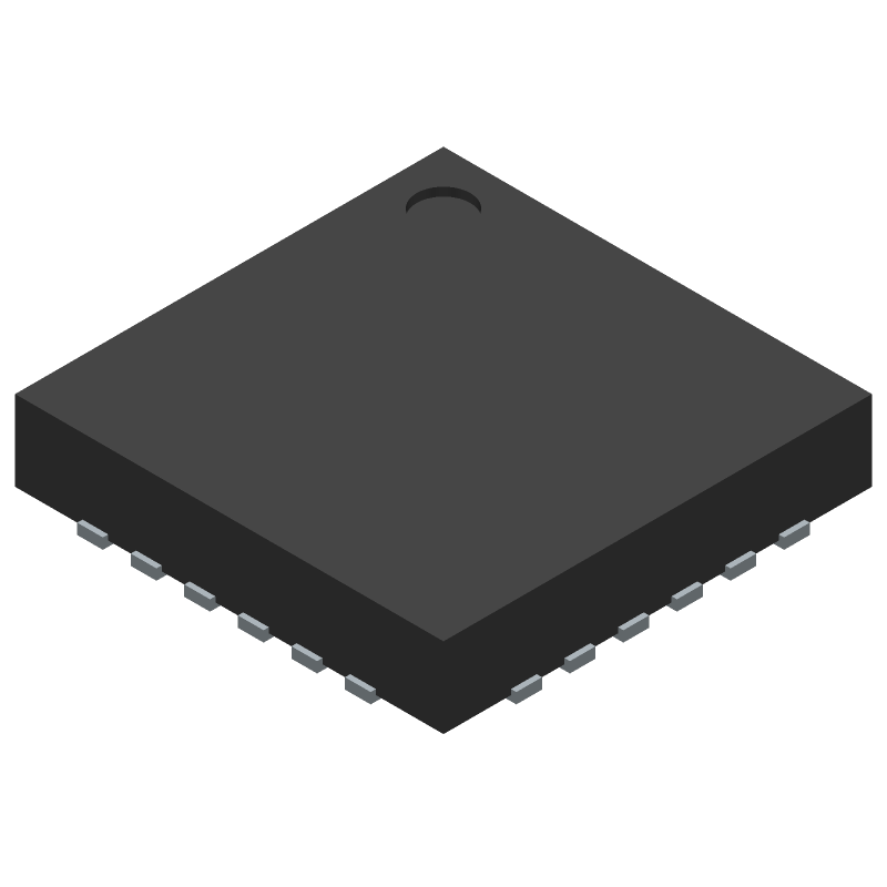
3D Model
Available Download Formats
By downloading CAD models, you agree to our Terms & Conditions and Privacy Policy
5.5 V, 5 A, High Efficiency, Step-Down DC-to-DC Regulators with Output Tracking
Tip: Data for a part may vary between manufacturers. You can filter for manufacturers on the top of the page next to the part image and part number.
ADP2165ACPZ-1.0-R7 by Analog Devices Inc is a Switching Regulator or Controller.
Switching Regulator or Controllers are under the broader part category of Power Circuits.
A power circuit delivers electricity in order to operate a load for an electronic device. Power circuits include transformers, generators and switches. Read more about Power Circuits on our Power Circuits part category page.
| Part # | Distributor | Description | Stock | Price | Buy | |
|---|---|---|---|---|---|---|
|
DISTI #
505-ADP2165ACPZ-1.0-R7CT-ND
|
DigiKey | IC REG BUCK 1V 5A 24LFCSP Min Qty: 1 Lead time: 10 Weeks Container: Digi-Reel®, Cut Tape (CT), Tape & Reel (TR) | Temporarily Out of Stock |
|
$2.9250 / $7.4500 | Buy Now |
|
DISTI #
584-ADP2165ACPZ1.0R7
|
Mouser Electronics | Switching Voltage Regulators High Eff Step Down Sync Reg 6V 5A RoHS: Compliant | 0 |
|
$3.2100 | Order Now |
|
|
Analog Devices Inc | High Eff Step Down Sync Reg 6V Min Qty: 1500 Package Multiple: 1500 | 1500 |
|
$2.2300 / $7.4500 | Buy Now |
|
DISTI #
69186301
|
Verical | Conv DC-DC 2.7V to 5.5V Synchronous Step Down Single-Out 1V 5A 24-Pin LFCSP EP T/R RoHS: Compliant Min Qty: 1500 Package Multiple: 1500 | Americas - 1500 |
|
$2.9434 | Buy Now |
|
|
Rochester Electronics | 5.5V, 5 A, High Efficiency, Step-Down DC-To-DC Regulator RoHS: Compliant Status: Active Min Qty: 1 | 797 |
|
$2.4600 / $3.0700 | Buy Now |
By downloading CAD models, you agree to our Terms & Conditions and Privacy Policy
|
|
ADP2165ACPZ-1.0-R7
Analog Devices Inc
Buy Now
Datasheet
|
Compare Parts:
ADP2165ACPZ-1.0-R7
Analog Devices Inc
5.5 V, 5 A, High Efficiency, Step-Down DC-to-DC Regulators with Output Tracking
|
| Pbfree Code | No | |
| Rohs Code | Yes | |
| Part Life Cycle Code | Active | |
| Ihs Manufacturer | ANALOG DEVICES INC | |
| Package Description | LFCSP-24 | |
| Pin Count | 24 | |
| Manufacturer Package Code | CP-24-15 | |
| Reach Compliance Code | compliant | |
| Samacsys Manufacturer | Analog Devices | |
| Analog IC - Other Type | SWITCHING REGULATOR | |
| Control Mode | CURRENT-MODE | |
| Control Technique | PULSE WIDTH MODULATION | |
| Input Voltage-Max | 5.5 V | |
| Input Voltage-Min | 2.7 V | |
| Input Voltage-Nom | 5 V | |
| JESD-30 Code | S-XQCC-N24 | |
| JESD-609 Code | e3 | |
| Length | 4 mm | |
| Moisture Sensitivity Level | 3 | |
| Number of Functions | 1 | |
| Number of Terminals | 24 | |
| Operating Temperature-Max | 125 °C | |
| Operating Temperature-Min | -40 °C | |
| Output Voltage-Nom | 1 V | |
| Package Body Material | UNSPECIFIED | |
| Package Code | HVQCCN | |
| Package Shape | SQUARE | |
| Package Style | CHIP CARRIER, HEAT SINK/SLUG, VERY THIN PROFILE | |
| Peak Reflow Temperature (Cel) | 260 | |
| Seated Height-Max | 0.8 mm | |
| Surface Mount | YES | |
| Switcher Configuration | BUCK | |
| Switching Frequency-Max | 1400 kHz | |
| Temperature Grade | AUTOMOTIVE | |
| Terminal Finish | Matte Tin (Sn) | |
| Terminal Form | NO LEAD | |
| Terminal Pitch | 0.5 mm | |
| Terminal Position | QUAD | |
| Time@Peak Reflow Temperature-Max (s) | 30 | |
| Width | 4 mm |
A good PCB layout for the ADP2165 involves keeping the input and output capacitors close to the device, using a solid ground plane, and minimizing the length of the input and output traces. Additionally, it's recommended to use a separate analog ground plane and to keep the power and ground traces separate.
To ensure stability, make sure to follow the recommended component values and PCB layout guidelines. Additionally, check that the input and output capacitors are of sufficient value and that the output voltage is within the recommended range. Also, ensure that the device is properly decoupled from the power supply and that the input voltage is clean and stable.
The maximum input voltage that can be applied to the ADP2165 is 6.5V. Exceeding this voltage can cause damage to the device. It's recommended to use a voltage regulator or other protection circuitry to ensure the input voltage remains within the recommended range.
The ADP2165 is rated for operation up to 125°C. However, the device's performance and reliability may be affected at high temperatures. It's recommended to follow the recommended operating conditions and to consider using thermal management techniques, such as heat sinks or thermal interfaces, to keep the device within its recommended operating temperature range.
The output voltage of the ADP2165 can be calculated using the formula: VOUT = (VIN x (1 + R1/R2)) - (IOUT x RDS(ON)). Where VIN is the input voltage, R1 and R2 are the feedback resistors, IOUT is the output current, and RDS(ON) is the on-resistance of the internal FET.