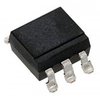
Part Details for ADP122ACPZ-2.8-R7 by Analog Devices Inc
Results Overview of ADP122ACPZ-2.8-R7 by Analog Devices Inc
- Distributor Offerings: (3 listings)
- Number of FFF Equivalents: (0 replacements)
- CAD Models: (Request Part)
- Number of Functional Equivalents: (1 option)
- Part Data Attributes: (Available)
- Reference Designs: (Not Available)
Tip: Data for a part may vary between manufacturers. You can filter for manufacturers on the top of the page next to the part image and part number.
ADP122ACPZ-2.8-R7 Information
ADP122ACPZ-2.8-R7 by Analog Devices Inc is a Linear Regulator IC.
Linear Regulator ICs are under the broader part category of Power Circuits.
A power circuit delivers electricity in order to operate a load for an electronic device. Power circuits include transformers, generators and switches. Read more about Power Circuits on our Power Circuits part category page.
Price & Stock for ADP122ACPZ-2.8-R7
| Part # | Distributor | Description | Stock | Price | Buy | |
|---|---|---|---|---|---|---|
|
|
Bristol Electronics | 894 |
|
RFQ | ||
|
|
Rochester Electronics | 5.5V Input, 300mA, Low Quiescent Current, CMOS Linear Regulator RoHS: Compliant Status: Obsolete Min Qty: 1 | 6200 |
|
$0.3686 / $0.5945 | Buy Now |
|
|
Vyrian | Regulators | 4256 |
|
RFQ |
Part Details for ADP122ACPZ-2.8-R7
ADP122ACPZ-2.8-R7 CAD Models
ADP122ACPZ-2.8-R7 Part Data Attributes
|
|
ADP122ACPZ-2.8-R7
Analog Devices Inc
Buy Now
Datasheet
|
Compare Parts:
ADP122ACPZ-2.8-R7
Analog Devices Inc
5.5 V Input, 300 mA, Low Quiescent Current, CMOS Linear Regulator, Fixed Output Voltage
|
| Pbfree Code | No | |
| Rohs Code | Yes | |
| Part Life Cycle Code | Obsolete | |
| Ihs Manufacturer | ANALOG DEVICES INC | |
| Part Package Code | SOIC | |
| Package Description | 2 X 2 MM, ROHS COMPLIANT, LFCSP-6 | |
| Pin Count | 6 | |
| Manufacturer Package Code | CP-6-3 | |
| Reach Compliance Code | compliant | |
| ECCN Code | EAR99 | |
| HTS Code | 8542.39.00.01 | |
| Samacsys Manufacturer | Analog Devices | |
| Dropout Voltage1-Max | 0.15 V | |
| Input Voltage-Max | 5.5 V | |
| Input Voltage-Min | 2.3 V | |
| JESD-30 Code | S-PDSO-N6 | |
| JESD-609 Code | e4 | |
| Length | 2 mm | |
| Moisture Sensitivity Level | 1 | |
| Number of Functions | 1 | |
| Number of Terminals | 6 | |
| Operating Temperature TJ-Max | 125 °C | |
| Operating Temperature TJ-Min | -40 °C | |
| Output Current1-Max | 0.3 A | |
| Output Voltage1-Max | 2.856 V | |
| Output Voltage1-Min | 2.744 V | |
| Output Voltage1-Nom | 2.8 V | |
| Package Body Material | PLASTIC/EPOXY | |
| Package Code | HVSON | |
| Package Equivalence Code | SOLCC6,.08,25 | |
| Package Shape | SQUARE | |
| Package Style | SMALL OUTLINE, HEAT SINK/SLUG, VERY THIN PROFILE | |
| Regulator Type | FIXED POSITIVE SINGLE OUTPUT LDO REGULATOR | |
| Seated Height-Max | 0.65 mm | |
| Surface Mount | YES | |
| Technology | CMOS | |
| Terminal Finish | NICKEL PALLADIUM GOLD | |
| Terminal Form | NO LEAD | |
| Terminal Pitch | 0.65 mm | |
| Terminal Position | DUAL | |
| Voltage Tolerance-Max | 2% | |
| Width | 2 mm |
Alternate Parts for ADP122ACPZ-2.8-R7
This table gives cross-reference parts and alternative options found for ADP122ACPZ-2.8-R7. The Form Fit Function (FFF) tab will give you the options that are more likely to serve as direct pin-to-pin alternates or drop-in parts. The Functional Equivalents tab will give you options that are likely to match the same function of ADP122ACPZ-2.8-R7, but it may not fit your design. Always verify details of parts you are evaluating, as these parts are offered as suggestions for what you are looking for and are not guaranteed.
| Part Number | Manufacturer | Composite Price | Description | Compare |
|---|---|---|---|---|
| LD6836CX4/27H | NXP Semiconductors | Check for Price | IC VREG 2.7 V FIXED POSITIVE LDO REGULATOR, 0.16 V DROPOUT, PBGA4, 0.76 X 0.76 MM, 0.47 MM HEIGHT, 0.40 MM PITCH, GREEN, WLCSP-4, Fixed Positive Single Output LDO Regulator | ADP122ACPZ-2.8-R7 vs LD6836CX4/27H |
ADP122ACPZ-2.8-R7 Frequently Asked Questions (FAQ)
-
For optimal thermal performance, it is recommended to have a solid copper plane under the device, and to use thermal vias to connect the plane to the thermal pad on the bottom of the package. Additionally, keeping the PCB layer stack-up symmetrical and using a thermal relief pattern around the device can help to reduce thermal resistance.
-
To ensure accurate output voltage regulation, it is essential to follow the recommended input and output capacitor selection, as well as the PCB layout guidelines. Additionally, the output voltage can be adjusted by using an external resistor divider network, and the device's output voltage tolerance can be improved by using a precision reference voltage.
-
Although the datasheet specifies a maximum input voltage of 5.5V, it is recommended to limit the input voltage to 5V to ensure reliable operation and to prevent damage to the device. Applying a voltage higher than 5V may cause the device to malfunction or fail.
-
The POR pin should be connected to a capacitor to ground to ensure a clean power-on reset. The EN pin should be connected to a logic signal or a pull-up resistor to enable the device. It is essential to follow the recommended timing and voltage levels for these pins to ensure proper device operation.
-
A low-ESR ceramic capacitor with a value of 1-10uF is recommended for input decoupling. The capacitor should be placed as close as possible to the device's input pin to minimize noise and ensure stable operation.
