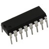
Part Details for ADG201ATQ by Analog Devices Inc
Results Overview of ADG201ATQ by Analog Devices Inc
- Distributor Offerings: (2 listings)
- Number of FFF Equivalents: (1 replacement)
- CAD Models: (Request Part)
- Number of Functional Equivalents: (10 options)
- Part Data Attributes: (Available)
- Reference Designs: (Not Available)
Tip: Data for a part may vary between manufacturers. You can filter for manufacturers on the top of the page next to the part image and part number.
ADG201ATQ Information
ADG201ATQ by Analog Devices Inc is a Multiplexer or Switch.
Multiplexers or Switches are under the broader part category of Signal Circuits.
A signal is an electronic means of transmitting information, either as an analog signal with continuous values or a digital signal with discrete values. Signals are used in various systems and networks. Read more about Signal Circuits on our Signal Circuits part category page.
Price & Stock for ADG201ATQ
| Part # | Distributor | Description | Stock | Price | Buy | |
|---|---|---|---|---|---|---|
|
|
Quest Components | SPST, 1 FUNC, 1 CHANNEL, CMOS, CDIP16 | 1 |
|
$24.0500 | Buy Now |
|
|
Vyrian | Peripheral ICs | 1307 |
|
RFQ |
Part Details for ADG201ATQ
ADG201ATQ CAD Models
ADG201ATQ Part Data Attributes
|
|
ADG201ATQ
Analog Devices Inc
Buy Now
Datasheet
|
Compare Parts:
ADG201ATQ
Analog Devices Inc
IC 1-CHANNEL, SGL POLE SGL THROW SWITCH, CDIP16, CERDIP-16, Multiplexer or Switch
|
| Rohs Code | No | |
| Part Life Cycle Code | Obsolete | |
| Ihs Manufacturer | ANALOG DEVICES INC | |
| Part Package Code | DIP | |
| Package Description | DIP, DIP16,.3 | |
| Pin Count | 16 | |
| Reach Compliance Code | not_compliant | |
| HTS Code | 8542.39.00.01 | |
| Analog IC - Other Type | SPST | |
| JESD-30 Code | R-GDIP-T16 | |
| JESD-609 Code | e0 | |
| Length | 19.495 mm | |
| Neg Supply Voltage-Nom (Vsup) | -15 V | |
| Normal Position | NC | |
| Number of Channels | 1 | |
| Number of Functions | 1 | |
| Number of Terminals | 16 | |
| Off-state Isolation-Nom | 80 dB | |
| On-state Resistance Match-Nom | 5 Ω | |
| On-state Resistance-Max (Ron) | 90 Ω | |
| Operating Temperature-Max | 125 °C | |
| Operating Temperature-Min | -55 °C | |
| Output | SEPARATE OUTPUT | |
| Package Body Material | CERAMIC, GLASS-SEALED | |
| Package Code | DIP | |
| Package Equivalence Code | DIP16,.3 | |
| Package Shape | RECTANGULAR | |
| Package Style | IN-LINE | |
| Qualification Status | Not Qualified | |
| Seated Height-Max | 4.572 mm | |
| Supply Voltage-Nom (Vsup) | 15 V | |
| Surface Mount | NO | |
| Switch-off Time-Max | 250 ns | |
| Switch-on Time-Max | 300 ns | |
| Switching | BREAK-BEFORE-MAKE | |
| Technology | CMOS | |
| Temperature Grade | MILITARY | |
| Terminal Finish | TIN LEAD | |
| Terminal Form | THROUGH-HOLE | |
| Terminal Pitch | 2.54 mm | |
| Terminal Position | DUAL | |
| Width | 7.62 mm |
Alternate Parts for ADG201ATQ
This table gives cross-reference parts and alternative options found for ADG201ATQ. The Form Fit Function (FFF) tab will give you the options that are more likely to serve as direct pin-to-pin alternates or drop-in parts. The Functional Equivalents tab will give you options that are likely to match the same function of ADG201ATQ, but it may not fit your design. Always verify details of parts you are evaluating, as these parts are offered as suggestions for what you are looking for and are not guaranteed.
| Part Number | Manufacturer | Composite Price | Description | Compare |
|---|---|---|---|---|
| ADG201AKNZ | Rochester Electronics LLC | Check for Price | SPST, 1 Func, 1 Channel, CMOS, PDIP16, PLASTIC, DIP-16 | ADG201ATQ vs ADG201AKNZ |
ADG201ATQ Frequently Asked Questions (FAQ)
-
The recommended power-up sequence is to apply VCC before applying the analog signal. This ensures that the internal circuitry is properly biased before the analog signal is applied.
-
To ensure correct switching at high frequencies, it is recommended to use a low-impedance power supply, minimize lead inductance, and use a low-capacitance layout. Additionally, the control signal should be a clean, low-impedance signal with a fast rise and fall time.
-
The maximum voltage that can be applied to the analog input pins is VCC + 0.3V. Exceeding this voltage can cause damage to the device.
-
To minimize the effect of charge injection, it is recommended to use a low-capacitance layout, minimize the distance between the switch and the load, and use a low-impedance load. Additionally, the control signal should be a clean, low-impedance signal with a fast rise and fall time.
-
The recommended operating temperature range for the ADG201ATQ is -40°C to +85°C. Operating the device outside of this range can affect its performance and reliability.
