-
Part Symbol
-
Footprint
-
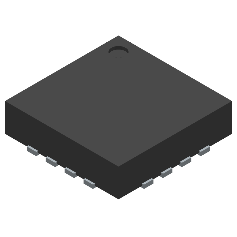
3D Model
Available Download Formats
By downloading CAD models, you agree to our Terms & Conditions and Privacy Policy

Ultrafast SiGe ECL Clock/Data Buffers
Tip: Data for a part may vary between manufacturers. You can filter for manufacturers on the top of the page next to the part image and part number.
ADCLK925BCPZ-WP by Analog Devices Inc is a Clock Driver.
Clock Drivers are under the broader part category of Logic Components.
Digital logic governs the behavior of signals in electronic circuits, enabling complex decisions based on simple binary inputs (yes/no). Logic components perform operations from these signals. Read more about Logic Components on our Logic part category page.
| Part # | Distributor | Description | Stock | Price | Buy | |
|---|---|---|---|---|---|---|
|
DISTI #
49AK8249
|
Newark | Ic, Clk/Data Buffer, 2.375V-3.63V, Lfcsp, Clock Ic Type:Clock Buffer, Frequency:7.5Ghz, No. Of Outputs:2Outputs, Supply Voltage Min:2.375V, Supply Voltage Max:3.63V, Clock Ic Case Style:Lfcsp-Ep, No. Of Pins:16Pins, Product Range:- Rohs Compliant: Yes |Analog Devices ADCLK925BCPZ-WP RoHS: Not Compliant Min Qty: 1 Package Multiple: 1 Date Code: 1 Container: Bulk | 10 |
|
$9.1900 / $15.3800 | Buy Now |
|
DISTI #
505-ADCLK925BCPZ-WP-ND
|
DigiKey | IC CLK BUFFER 1:2 7.5GHZ 16LFCSP Min Qty: 1 Lead time: 33 Weeks Container: Tray |
29 In Stock |
|
$8.8500 / $16.4100 | Buy Now |
|
DISTI #
584-ADCLK925BCPZ-WP
|
Mouser Electronics | Clock Buffer 1:2 ECL, 7 Gbpps CLOCK/DATA BUFFERS RoHS: Compliant | 428 |
|
$9.1900 / $15.3800 | Buy Now |
|
|
Analog Devices Inc | 1:2 ECL, 7 Gbpps CLOCK/DATA BU Min Qty: 1 Package Multiple: 50 | 5176 |
|
$6.5800 / $16.4100 | Buy Now |
|
DISTI #
26617550
|
Verical | Clock Fanout Buffer 2-OUT 1-IN 1:2 16-Pin LFCSP EP Tray RoHS: Compliant Min Qty: 50 Package Multiple: 50 | Americas - 5150 |
|
$8.7570 | Buy Now |
|
DISTI #
ADCLK925BCPZ-WP
|
Richardson RFPD | CLOCK BUFFERS RoHS: Compliant Min Qty: 50 | 0 |
|
$9.2600 / $9.8900 | Buy Now |
|
|
LCSC | 2.375V3.63V 7.5GHz LFCSP-16-VQ(3x3) Clock Buffers Drivers Distributors ROHS | 10 |
|
$11.0422 / $13.5918 | Buy Now |
By downloading CAD models, you agree to our Terms & Conditions and Privacy Policy
|
|
ADCLK925BCPZ-WP
Analog Devices Inc
Buy Now
Datasheet
|
Compare Parts:
ADCLK925BCPZ-WP
Analog Devices Inc
Ultrafast SiGe ECL Clock/Data Buffers
|
| Pbfree Code | No | |
| Rohs Code | Yes | |
| Part Life Cycle Code | Active | |
| Ihs Manufacturer | ANALOG DEVICES INC | |
| Part Package Code | QFN | |
| Package Description | LFCSP-16 | |
| Pin Count | 16 | |
| Manufacturer Package Code | CP-16-27 | |
| Reach Compliance Code | compliant | |
| ECCN Code | EAR99 | |
| HTS Code | 8542.39.00.01 | |
| Samacsys Manufacturer | Analog Devices | |
| Family | 925 | |
| Input Conditioning | DIFFERENTIAL | |
| JESD-30 Code | S-XQCC-N16 | |
| JESD-609 Code | e3 | |
| Length | 3 mm | |
| Logic IC Type | LOW SKEW CLOCK DRIVER | |
| Moisture Sensitivity Level | 3 | |
| Number of Functions | 1 | |
| Number of Inverted Outputs | ||
| Number of Terminals | 16 | |
| Number of True Outputs | 2 | |
| Operating Temperature-Max | 125 °C | |
| Operating Temperature-Min | -40 °C | |
| Package Body Material | UNSPECIFIED | |
| Package Code | HVQCCN | |
| Package Equivalence Code | LCC16,.12SQ,20 | |
| Package Shape | SQUARE | |
| Package Style | CHIP CARRIER, HEAT SINK/SLUG, VERY THIN PROFILE | |
| Peak Reflow Temperature (Cel) | 260 | |
| Power Supply Current-Max (ICC) | 97 mA | |
| Prop. Delay@Nom-Sup | 0.125 ns | |
| Propagation Delay (tpd) | 0.125 ns | |
| Same Edge Skew-Max (tskwd) | 0.01 ns | |
| Seated Height-Max | 0.8 mm | |
| Supply Voltage-Max (Vsup) | 3.63 V | |
| Supply Voltage-Min (Vsup) | 2.375 V | |
| Supply Voltage-Nom (Vsup) | 2.5 V | |
| Surface Mount | YES | |
| Technology | BIPOLAR | |
| Terminal Finish | Matte Tin (Sn) | |
| Terminal Form | NO LEAD | |
| Terminal Pitch | 0.5 mm | |
| Terminal Position | QUAD | |
| Time@Peak Reflow Temperature-Max (s) | 30 | |
| Width | 3 mm |
The recommended power-up sequence is to apply VCC first, followed by VEE, and then the input clock signal. This ensures proper device operation and prevents potential latch-up conditions.
To optimize the output clock signal quality and reduce jitter, ensure that the input clock signal is clean and has minimal jitter. Also, use a low-jitter crystal oscillator as the input clock source, and consider using a clock conditioning circuit or a phase-locked loop (PLL) to further reduce jitter.
The maximum frequency of operation for the ADCLK925BCPZ-WP is 250 MHz. However, the actual maximum frequency may vary depending on the specific application, board layout, and environmental conditions.
To ensure proper thermal management, ensure good airflow around the device, use a heat sink if necessary, and avoid blocking the airflow around the device. Also, follow the recommended PCB layout guidelines to minimize thermal resistance.
The recommended layout and routing for the ADCLK925BCPZ-WP involves keeping the input clock signal traces short and shielded, using a solid ground plane, and minimizing the distance between the device and the output load. Also, avoid crossing clock signal traces over other signals or power planes.