-
Part Symbol
-
Footprint
-
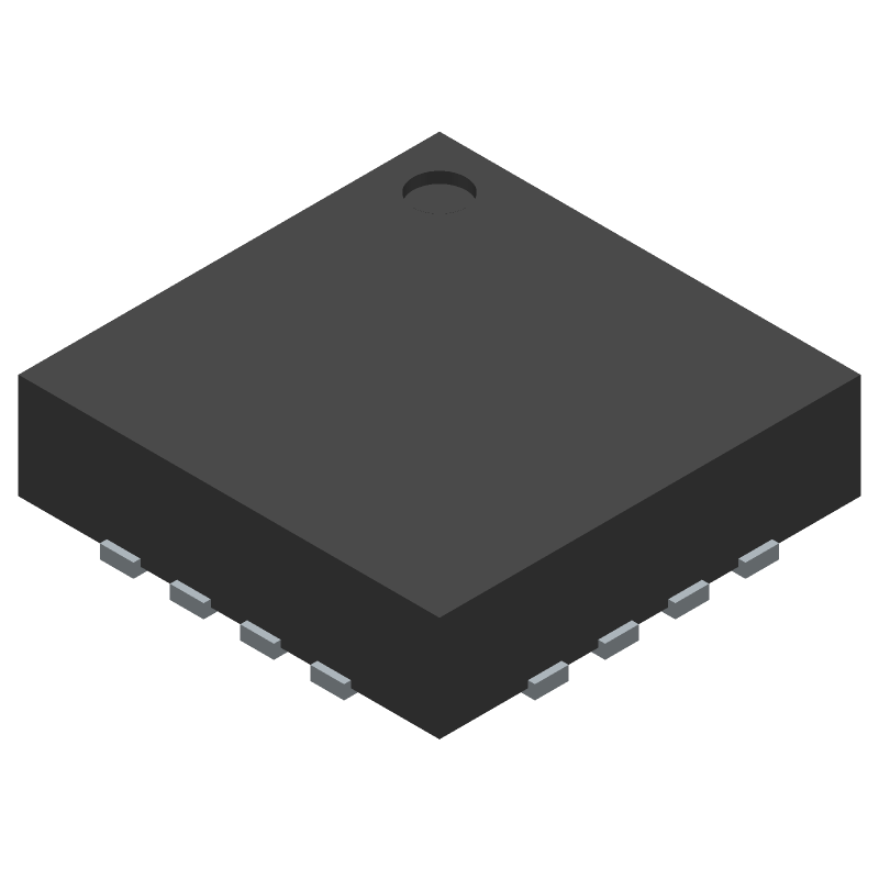
3D Model
Available Download Formats
By downloading CAD models, you agree to our Terms & Conditions and Privacy Policy

Ultrafast, SiGe, Open-Collector HVDS Clock/Data Buffer
Tip: Data for a part may vary between manufacturers. You can filter for manufacturers on the top of the page next to the part image and part number.
ADCLK914BCPZ-R7 by Analog Devices Inc is a Buffer Amplifier.
Buffer Amplifiers are under the broader part category of Amplifier Circuits.
Amplifier circuits use external power to increase the amplitude of an input signal. They can be used to perform linear amplifications or logarithmic functions. Read more about Amplifier Circuits on our Amplifier Circuits part category page.
| Part # | Distributor | Description | Stock | Price | Buy | |
|---|---|---|---|---|---|---|
|
DISTI #
47AK1227
|
Newark | Clock/Data Buffer, 7.5Ghz, Lfcsp-Ep, Clock Ic Type:Clock & Data Buffer, Frequency:7.5Ghz, No. Of Outputs:1Outputs, Supply Voltage Min:2.97V, Supply Voltage Max:3.63V, Clock Ic Case Style:Lfcsp-Ep, No. Of Pins:16Pins, Product Range:- Rohs Compliant: Yes |Analog Devices ADCLK914BCPZ-R7 RoHS: Compliant Min Qty: 1 Package Multiple: 1 Date Code: 1 Container: Cut Tape | 605 |
|
$11.2500 / $16.5800 | Buy Now |
|
DISTI #
505-ADCLK914BCPZ-R7CT-ND
|
DigiKey | IC CLK BUFFER 1:1 7.5GHZ 16LFCSP Min Qty: 1 Lead time: 10 Weeks Container: Digi-Reel®, Tape & Reel (TR), Cut Tape (CT) |
2023 In Stock |
|
$11.2500 / $19.7200 | Buy Now |
|
DISTI #
584-ADCLK914BCPZ-R7
|
Mouser Electronics | Clock Buffer 1:1 ECL, 3 Gbpps CLOCK/DATA BUFFERS RoHS: Compliant | 2331 |
|
$11.2400 / $16.4900 | Buy Now |
|
DISTI #
V72:2272_06217762
|
Arrow Electronics | Clock Fanout Buffer 1-OUT 1-IN 1:1 16-Pin LFCSP EP T/R RoHS: Compliant Min Qty: 1 Package Multiple: 1 Lead time: 10 Weeks Date Code: 2211 Container: Cut Strips | Americas - 13 |
|
$12.0800 / $13.9500 | Buy Now |
|
|
Analog Devices Inc | 1:1 ECL, 3 Gbpps CLOCK/DATA BU Min Qty: 1 Package Multiple: 1500 | 1905 |
|
$8.5500 / $19.7200 | Buy Now |
|
DISTI #
26617547
|
Verical | Clock Fanout Buffer 1-OUT 1-IN 1:1 16-Pin LFCSP EP T/R RoHS: Compliant Min Qty: 1500 Package Multiple: 1500 | Americas - 1500 |
|
$11.1317 | Buy Now |
|
|
Quest Components | BUFFER AMPLIFIER, 1 FUNC, BICMOS | 71 |
|
$12.9500 / $15.7500 | Buy Now |
|
|
Rochester Electronics | Buffer Amplifier, BICMOS RoHS: Compliant Status: Active Min Qty: 1 | 4498 |
|
$9.4700 / $11.8400 | Buy Now |
|
DISTI #
ADCLK914BCPZ
|
Richardson RFPD | CLOCK MODULE RoHS: Compliant Min Qty: 1 | 55 |
|
$11.7700 / $13.5000 | Buy Now |
|
|
Win Source Electronics | IC CLK BUFFER 1:1 7.5GHZ 16LFCSP | 1500 |
|
$27.2253 / $40.8379 | Buy Now |
By downloading CAD models, you agree to our Terms & Conditions and Privacy Policy
|
|
ADCLK914BCPZ-R7
Analog Devices Inc
Buy Now
Datasheet
|
Compare Parts:
ADCLK914BCPZ-R7
Analog Devices Inc
Ultrafast, SiGe, Open-Collector HVDS Clock/Data Buffer
|
| Pbfree Code | No | |
| Rohs Code | Yes | |
| Part Life Cycle Code | Active | |
| Ihs Manufacturer | ANALOG DEVICES INC | |
| Part Package Code | QFN | |
| Package Description | LFCSP-16 | |
| Pin Count | 16 | |
| Manufacturer Package Code | CP-16-22 | |
| Reach Compliance Code | compliant | |
| ECCN Code | EAR99 | |
| HTS Code | 8542.39.00.01 | |
| Samacsys Manufacturer | Analog Devices | |
| Amplifier Type | BUFFER | |
| JESD-30 Code | S-XQCC-N16 | |
| JESD-609 Code | e3 | |
| Length | 3 mm | |
| Moisture Sensitivity Level | 3 | |
| Number of Functions | 1 | |
| Number of Terminals | 16 | |
| Operating Temperature-Max | 125 °C | |
| Operating Temperature-Min | -40 °C | |
| Package Body Material | UNSPECIFIED | |
| Package Code | HVQCCN | |
| Package Shape | SQUARE | |
| Package Style | CHIP CARRIER | |
| Peak Reflow Temperature (Cel) | 260 | |
| Qualification Status | Not Qualified | |
| Seated Height-Max | 0.9 mm | |
| Supply Voltage Limit-Max | 6 V | |
| Supply Voltage-Nom (Vsup) | 3.3 V | |
| Surface Mount | YES | |
| Technology | BICMOS | |
| Temperature Grade | AUTOMOTIVE | |
| Terminal Finish | Matte Tin (Sn) | |
| Terminal Form | NO LEAD | |
| Terminal Pitch | 0.5 mm | |
| Terminal Position | QUAD | |
| Time@Peak Reflow Temperature-Max (s) | 40 | |
| Width | 3 mm |
The recommended power-up sequence is to apply VCC first, followed by VEE, and then the input clock signal. This ensures proper device operation and prevents potential latch-up conditions.
To minimize jitter and noise, keep the clock signal traces short and away from noisy signals, use a solid ground plane, and decouple the power supplies with capacitors. Also, consider using a clock-specific layout guideline, such as the 'star' or 'hub' configuration, to reduce clock signal skew.
The ADCLK914BCPZ-R7 can handle clock frequencies up to 1.4 GHz, but the maximum frequency may vary depending on the specific application and output load. It's recommended to consult the datasheet and application notes for more information.
The ADCLK914BCPZ-R7 has a programmable output frequency divider, which can be configured using the SDATA and SCLK pins. Consult the datasheet and application notes for specific configuration details and examples.
The typical power consumption of the ADCLK914BCPZ-R7 is around 350 mW, but this can vary depending on the specific application, output frequency, and load conditions. Consult the datasheet for more information on power consumption and thermal considerations.