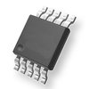
Part Details for ADC104S101CIMMX by Texas Instruments
Results Overview of ADC104S101CIMMX by Texas Instruments
- Distributor Offerings: (1 listing)
- Number of FFF Equivalents: (3 replacements)
- CAD Models: (Request Part)
- Number of Functional Equivalents: (3 options)
- Part Data Attributes: (Available)
- Reference Designs: (Not Available)
Tip: Data for a part may vary between manufacturers. You can filter for manufacturers on the top of the page next to the part image and part number.
ADC104S101CIMMX Information
ADC104S101CIMMX by Texas Instruments is an Analog to Digital Converter.
Analog to Digital Converters are under the broader part category of Converters.
A converter is an electrical circuit that transforms electric energy into a different form that will support a elecrical load needed by a device. Read more about Converters on our Converters part category page.
Price & Stock for ADC104S101CIMMX
| Part # | Distributor | Description | Stock | Price | Buy | |
|---|---|---|---|---|---|---|
|
|
Vyrian | Peripheral ICs | 626 |
|
RFQ |
Part Details for ADC104S101CIMMX
ADC104S101CIMMX CAD Models
ADC104S101CIMMX Part Data Attributes
|
|
ADC104S101CIMMX
Texas Instruments
Buy Now
Datasheet
|
Compare Parts:
ADC104S101CIMMX
Texas Instruments
4-CH 10-BIT SUCCESSIVE APPROXIMATION ADC, SERIAL ACCESS, PDSO10, MSOP-10
|
| Pbfree Code | No | |
| Rohs Code | No | |
| Part Life Cycle Code | Obsolete | |
| Ihs Manufacturer | TEXAS INSTRUMENTS INC | |
| Part Package Code | MSOP | |
| Package Description | MSOP-10 | |
| Pin Count | 10 | |
| Reach Compliance Code | not_compliant | |
| HTS Code | 8542.39.00.01 | |
| Analog Input Voltage-Max | 5.25 V | |
| Analog Input Voltage-Min | ||
| Conversion Time-Max | 0.8125 µs | |
| Converter Type | ADC, SUCCESSIVE APPROXIMATION | |
| JESD-30 Code | S-PDSO-G10 | |
| JESD-609 Code | e0 | |
| Length | 3 mm | |
| Linearity Error-Max (EL) | 0.0684% | |
| Moisture Sensitivity Level | 1 | |
| Number of Analog In Channels | 4 | |
| Number of Bits | 10 | |
| Number of Functions | 1 | |
| Number of Terminals | 10 | |
| Operating Temperature-Max | 85 °C | |
| Operating Temperature-Min | -40 °C | |
| Output Bit Code | BINARY | |
| Output Format | SERIAL | |
| Package Body Material | PLASTIC/EPOXY | |
| Package Code | TSSOP | |
| Package Equivalence Code | TSSOP10,.19,20 | |
| Package Shape | SQUARE | |
| Package Style | SMALL OUTLINE, THIN PROFILE, SHRINK PITCH | |
| Peak Reflow Temperature (Cel) | 260 | |
| Qualification Status | Not Qualified | |
| Sample Rate | 1 MHz | |
| Sample and Hold / Track and Hold | TRACK | |
| Seated Height-Max | 1.09 mm | |
| Supply Voltage-Nom | 3 V | |
| Surface Mount | YES | |
| Technology | CMOS | |
| Temperature Grade | INDUSTRIAL | |
| Terminal Finish | TIN LEAD | |
| Terminal Form | GULL WING | |
| Terminal Pitch | 0.5 mm | |
| Terminal Position | DUAL | |
| Width | 3 mm |
Alternate Parts for ADC104S101CIMMX
This table gives cross-reference parts and alternative options found for ADC104S101CIMMX. The Form Fit Function (FFF) tab will give you the options that are more likely to serve as direct pin-to-pin alternates or drop-in parts. The Functional Equivalents tab will give you options that are likely to match the same function of ADC104S101CIMMX, but it may not fit your design. Always verify details of parts you are evaluating, as these parts are offered as suggestions for what you are looking for and are not guaranteed.
| Part Number | Manufacturer | Composite Price | Description | Compare |
|---|---|---|---|---|
| ADC104S101CIMM/NOPB | Texas Instruments | $2.6068 | 4 Channel 500 ksps to 1 Msps, 10-Bit A/D Converter 10-VSSOP -40 to 85 | ADC104S101CIMMX vs ADC104S101CIMM/NOPB |
| ADC104S101CIMMX | National Semiconductor Corporation | Check for Price | IC 4-CH 10-BIT SUCCESSIVE APPROXIMATION ADC, SERIAL ACCESS, PDSO10, MSOP-10, Analog to Digital Converter | ADC104S101CIMMX vs ADC104S101CIMMX |
| ADC104S101CIMM | National Semiconductor Corporation | Check for Price | IC 4-CH 10-BIT SUCCESSIVE APPROXIMATION ADC, SERIAL ACCESS, PDSO10, MSOP-10, Analog to Digital Converter | ADC104S101CIMMX vs ADC104S101CIMM |
ADC104S101CIMMX Frequently Asked Questions (FAQ)
-
Texas Instruments provides a layout and routing guide in the application note SLAA523, which recommends a symmetrical layout, minimal trace length, and proper decoupling to reduce noise and ensure accurate conversions.
-
It is recommended to use a low-jitter clock source, such as a crystal oscillator, and to use a clock buffer or repeater to reduce clock skew and jitter. Additionally, the clock signal should be routed close to the ADC and away from noisy signals.
-
The recommended power-up sequence is to power up the analog supply (AVDD) first, followed by the digital supply (DVDD), and then the clock signal. This ensures that the ADC is properly biased and configured before the clock signal is applied.
-
The ADC104S101CIMMX has an internal calibration feature that can be used to adjust the offset and gain errors. The calibration process involves applying a known input voltage and reading the corresponding digital output code, and then adjusting the internal calibration registers to minimize the error.
-
The maximum input voltage range for the ADC104S101CIMMX is 0 to VREF (typically 2.5V or 5V). To handle overvoltage conditions, it is recommended to use external voltage limiting circuits, such as voltage dividers or clamping diodes, to prevent damage to the ADC.
