-
Part Symbol
-
Footprint
-
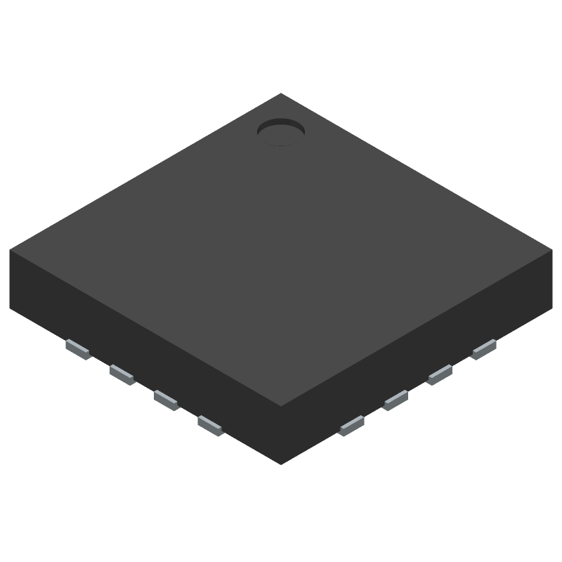
3D Model
Available Download Formats
By downloading CAD models, you agree to our Terms & Conditions and Privacy Policy

Ultralow Distortion, Low Power, Low Noise, High Speed Op Amp
Tip: Data for a part may vary between manufacturers. You can filter for manufacturers on the top of the page next to the part image and part number.
ADA4857-2YCPZ-R2 by Analog Devices Inc is an Operational Amplifier.
Operational Amplifiers are under the broader part category of Amplifier Circuits.
Amplifier circuits use external power to increase the amplitude of an input signal. They can be used to perform linear amplifications or logarithmic functions. Read more about Amplifier Circuits on our Amplifier Circuits part category page.
| Part # | Distributor | Description | Stock | Price | Buy | |
|---|---|---|---|---|---|---|
|
DISTI #
ADA4857-2YCPZ-R2CT-ND
|
DigiKey | IC OPAMP VFB 2 CIRCUIT 16LFCSP Lead time: 7 Weeks Container: Digi-Reel®, Cut Tape (CT), Tape & Reel (TR) | Limited Supply - Call |
|
Buy Now | |
|
|
Vyrian | Peripheral ICs | 670 |
|
RFQ |
By downloading CAD models, you agree to our Terms & Conditions and Privacy Policy
|
|
ADA4857-2YCPZ-R2
Analog Devices Inc
Buy Now
Datasheet
|
Compare Parts:
ADA4857-2YCPZ-R2
Analog Devices Inc
Ultralow Distortion, Low Power, Low Noise, High Speed Op Amp
|
| Pbfree Code | No | |
| Rohs Code | Yes | |
| Part Life Cycle Code | Obsolete | |
| Ihs Manufacturer | ANALOG DEVICES INC | |
| Part Package Code | QFN | |
| Package Description | LFCSP-16 | |
| Pin Count | 16 | |
| Manufacturer Package Code | CP-16-23 | |
| Reach Compliance Code | unknown | |
| ECCN Code | EAR99 | |
| HTS Code | 8542.33.00.01 | |
| Samacsys Manufacturer | Analog Devices | |
| Amplifier Type | OPERATIONAL AMPLIFIER | |
| Architecture | VOLTAGE-FEEDBACK | |
| Average Bias Current-Max (IIB) | 3.3 µA | |
| Bias Current-Max (IIB) @25C | 3.3 µA | |
| Common-mode Reject Ratio-Nom | 86 dB | |
| Frequency Compensation | YES | |
| Input Offset Voltage-Max | 4.5 µV | |
| JESD-30 Code | S-XQCC-N16 | |
| JESD-609 Code | e3 | |
| Length | 4 mm | |
| Low-Bias | NO | |
| Low-Offset | NO | |
| Micropower | NO | |
| Moisture Sensitivity Level | 3 | |
| Neg Supply Voltage Limit-Max | -5.5 V | |
| Neg Supply Voltage-Nom (Vsup) | -5 V | |
| Number of Functions | 2 | |
| Number of Terminals | 16 | |
| Operating Temperature-Max | 125 °C | |
| Operating Temperature-Min | -40 °C | |
| Package Body Material | UNSPECIFIED | |
| Package Code | HVQCCN | |
| Package Equivalence Code | LCC16,.16SQ,20 | |
| Package Shape | SQUARE | |
| Package Style | CHIP CARRIER, HEAT SINK/SLUG, VERY THIN PROFILE | |
| Packing Method | TR | |
| Peak Reflow Temperature (Cel) | 260 | |
| Power | NO | |
| Programmable Power | NO | |
| Qualification Status | Not Qualified | |
| Seated Height-Max | 1 mm | |
| Slew Rate-Nom | 2800 V/us | |
| Supply Current-Max | 5.5 mA | |
| Supply Voltage Limit-Max | 5.5 V | |
| Supply Voltage-Nom (Vsup) | 5 V | |
| Surface Mount | YES | |
| Technology | BIPOLAR | |
| Temperature Grade | AUTOMOTIVE | |
| Terminal Finish | MATTE TIN | |
| Terminal Form | NO LEAD | |
| Terminal Pitch | 0.65 mm | |
| Terminal Position | QUAD | |
| Unity Gain BW-Nom | 595000 | |
| Wideband | YES | |
| Width | 4 mm |
This table gives cross-reference parts and alternative options found for ADA4857-2YCPZ-R2. The Form Fit Function (FFF) tab will give you the options that are more likely to serve as direct pin-to-pin alternates or drop-in parts. The Functional Equivalents tab will give you options that are likely to match the same function of ADA4857-2YCPZ-R2, but it may not fit your design. Always verify details of parts you are evaluating, as these parts are offered as suggestions for what you are looking for and are not guaranteed.
| Part Number | Manufacturer | Composite Price | Description | Compare |
|---|---|---|---|---|
| ADA4857-2YCPZ-RL | Analog Devices Inc | Check for Price | Ultralow Distortion, Low Power, Low Noise, High Speed Op Amp | ADA4857-2YCPZ-R2 vs ADA4857-2YCPZ-RL |
A good PCB layout for the ADA4857-2YCPZ-R2 involves keeping the input and output traces short and away from each other, using a solid ground plane, and placing decoupling capacitors close to the device. A 4-layer PCB with a dedicated ground plane is recommended.
To ensure the ADA4857-2YCPZ-R2 operates within the specified temperature range, make sure to provide adequate heat sinking, avoid overheating, and keep the device away from high-temperature sources. The device is rated for operation from -40°C to +125°C.
The recommended power-up sequence for the ADA4857-2YCPZ-R2 is to apply the power supply voltage (VCC) before applying the input signals. This ensures that the device is properly biased and configured before signal processing begins.
To handle ESD protection for the ADA4857-2YCPZ-R2, use ESD protection devices such as TVS diodes or ESD protection arrays on the input and output pins. Follow proper handling and storage procedures to prevent ESD damage.
The recommended input and output termination for the ADA4857-2YCPZ-R2 depends on the specific application. For most applications, a 50Ω termination is recommended for the input and output pins. However, the optimal termination may vary depending on the specific signal frequencies and impedances involved.