-
Part Symbol
-
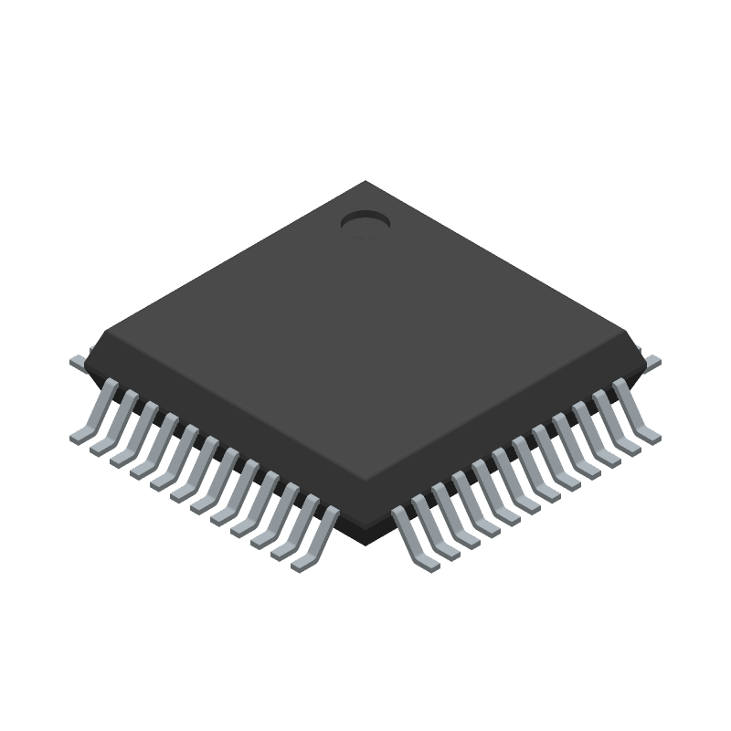
Footprint
-
3D Model
Available Download Formats
By downloading CAD models, you agree to our Terms & Conditions and Privacy Policy

Complete 10-Bit, 40 MHz CCD Signal Processor
Tip: Data for a part may vary between manufacturers. You can filter for manufacturers on the top of the page next to the part image and part number.
| Part # | Distributor | Description | Stock | Price | Buy | |
|---|---|---|---|---|---|---|
|
DISTI #
2156-AD9840AJSTZRL-ND
|
DigiKey | IC CCD SIGNAL PROC 10BIT 48LQFP Min Qty: 29 Lead time: 10 Weeks Container: Bulk MARKETPLACE PRODUCT |
6200 In Stock |
|
$10.6900 | Buy Now |
|
DISTI #
AD9840AJSTZRLTR-ND
|
DigiKey | IC CCD SIGNAL PROC 10BIT 48LQFP Min Qty: 29 Lead time: 10 Weeks Container: Tape & Reel (TR) | Temporarily Out of Stock |
|
$9.7875 | Buy Now |
|
DISTI #
584-AD9840AJSTZR
|
Mouser Electronics | Analog Front End - AFE 10B 40 MHz AFE NO PXGA RoHS: Compliant | 0 |
|
$9.7800 | Order Now |
|
|
Rochester Electronics | Complete 10-Bit 40 MSPS CCD Signal Processor RoHS: Compliant Status: Active Min Qty: 1 | 6200 |
|
$8.2400 / $10.3000 | Buy Now |
By downloading CAD models, you agree to our Terms & Conditions and Privacy Policy
|
|
AD9840AJSTZRL
Analog Devices Inc
Buy Now
Datasheet
|
Compare Parts:
AD9840AJSTZRL
Analog Devices Inc
Complete 10-Bit, 40 MHz CCD Signal Processor
|
| Pbfree Code | No | |
| Rohs Code | Yes | |
| Part Life Cycle Code | Active | |
| Ihs Manufacturer | ANALOG DEVICES INC | |
| Part Package Code | QFP | |
| Package Description | PLASTIC, LQFP-48 | |
| Pin Count | 48 | |
| Manufacturer Package Code | ST-48 | |
| Reach Compliance Code | compliant | |
| ECCN Code | EAR99 | |
| HTS Code | 8542.31.00.01 | |
| Samacsys Manufacturer | Analog Devices | |
| Consumer IC Type | CONSUMER CIRCUIT | |
| JESD-30 Code | S-PQFP-G48 | |
| JESD-609 Code | e3 | |
| Length | 7 mm | |
| Moisture Sensitivity Level | 3 | |
| Number of Functions | 1 | |
| Number of Terminals | 48 | |
| Operating Temperature-Max | 85 °C | |
| Operating Temperature-Min | -20 °C | |
| Package Body Material | PLASTIC/EPOXY | |
| Package Code | LFQFP | |
| Package Shape | SQUARE | |
| Package Style | FLATPACK, LOW PROFILE, FINE PITCH | |
| Peak Reflow Temperature (Cel) | 260 | |
| Qualification Status | Not Qualified | |
| Seated Height-Max | 1.6 mm | |
| Supply Voltage-Max (Vsup) | 3.6 V | |
| Supply Voltage-Min (Vsup) | 2.7 V | |
| Surface Mount | YES | |
| Temperature Grade | OTHER | |
| Terminal Finish | Matte Tin (Sn) | |
| Terminal Form | GULL WING | |
| Terminal Pitch | 0.5 mm | |
| Terminal Position | QUAD | |
| Time@Peak Reflow Temperature-Max (s) | 30 | |
| Width | 7 mm |
This table gives cross-reference parts and alternative options found for AD9840AJSTZRL. The Form Fit Function (FFF) tab will give you the options that are more likely to serve as direct pin-to-pin alternates or drop-in parts. The Functional Equivalents tab will give you options that are likely to match the same function of AD9840AJSTZRL, but it may not fit your design. Always verify details of parts you are evaluating, as these parts are offered as suggestions for what you are looking for and are not guaranteed.
| Part Number | Manufacturer | Composite Price | Description | Compare |
|---|---|---|---|---|
| AD9840AJSTRL | Analog Devices Inc | Check for Price | IC SPECIALTY CONSUMER CIRCUIT, PQFP48, PLASTIC, LQFP-48, Consumer IC:Other | AD9840AJSTZRL vs AD9840AJSTRL |
| AD9840AJSTZ | Analog Devices Inc | Check for Price | Complete 10-Bit, 40 MHz CCD Signal Processor | AD9840AJSTZRL vs AD9840AJSTZ |
A 4-layer PCB with a solid ground plane, separate analog and digital power planes, and careful routing of sensitive signals is recommended. Refer to the AD9840 evaluation board layout as a reference.
Use a high-quality clock source with low jitter (<100 ps RMS) and ensure the clock signal is properly terminated. The AD9840 has an internal clock buffer, but an external clock buffer (e.g., ADCLK925) can further improve jitter performance.
The maximum cable length for the LVDS outputs depends on the specific application and signal integrity requirements. As a general guideline, keep cable lengths below 10 inches (25 cm) to ensure signal integrity and minimize signal degradation.
The AD9840 can be configured for different data formats using the MODE pins (MODE0-MODE3). Refer to the datasheet's 'Mode Selection' section for specific pin configurations and settings.
To power down the AD9840, follow this sequence: 1) disable the clock input, 2) set the PDWN pin high, and 3) reduce the power supply voltage to 0 V. This sequence ensures proper shutdown and minimizes power consumption.