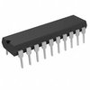
Part Details for AD977BN by Analog Devices Inc
Results Overview of AD977BN by Analog Devices Inc
- Distributor Offerings: (0 listings)
- Number of FFF Equivalents: (1 replacement)
- CAD Models: (Request Part)
- Number of Functional Equivalents: (10 options)
- Part Data Attributes: (Available)
- Reference Designs: (Not Available)
Tip: Data for a part may vary between manufacturers. You can filter for manufacturers on the top of the page next to the part image and part number.
AD977BN Information
AD977BN by Analog Devices Inc is an Analog to Digital Converter.
Analog to Digital Converters are under the broader part category of Converters.
A converter is an electrical circuit that transforms electric energy into a different form that will support a elecrical load needed by a device. Read more about Converters on our Converters part category page.
Part Details for AD977BN
AD977BN CAD Models
AD977BN Part Data Attributes
|
|
AD977BN
Analog Devices Inc
Buy Now
Datasheet
|
Compare Parts:
AD977BN
Analog Devices Inc
IC 3-CH 16-BIT SUCCESSIVE APPROXIMATION ADC, SERIAL ACCESS, PDIP20, 0.300 INCH, PLASTIC, DIP-20, Analog to Digital Converter
|
| Rohs Code | No | |
| Part Life Cycle Code | Obsolete | |
| Ihs Manufacturer | ANALOG DEVICES INC | |
| Part Package Code | DIP | |
| Package Description | DIP, DIP20,.3 | |
| Pin Count | 20 | |
| Reach Compliance Code | not_compliant | |
| HTS Code | 8542.39.00.01 | |
| Analog Input Voltage-Max | 10 V | |
| Analog Input Voltage-Min | -10 V | |
| Conversion Time-Max | 8 µs | |
| Converter Type | ADC, SUCCESSIVE APPROXIMATION | |
| JESD-30 Code | R-PDIP-T20 | |
| JESD-609 Code | e0 | |
| Length | 25.2 mm | |
| Linearity Error-Max (EL) | 0.0031% | |
| Number of Analog In Channels | 3 | |
| Number of Bits | 16 | |
| Number of Functions | 1 | |
| Number of Terminals | 20 | |
| Operating Temperature-Max | 85 °C | |
| Operating Temperature-Min | -40 °C | |
| Output Bit Code | BINARY, 2'S COMPLEMENT BINARY | |
| Output Format | SERIAL | |
| Package Body Material | PLASTIC/EPOXY | |
| Package Code | DIP | |
| Package Equivalence Code | DIP20,.3 | |
| Package Shape | RECTANGULAR | |
| Package Style | IN-LINE | |
| Qualification Status | Not Qualified | |
| Sample Rate | 0.1 MHz | |
| Seated Height-Max | 5.33 mm | |
| Supply Voltage-Nom | 5 V | |
| Surface Mount | NO | |
| Technology | BICMOS | |
| Temperature Grade | INDUSTRIAL | |
| Terminal Finish | TIN LEAD | |
| Terminal Form | THROUGH-HOLE | |
| Terminal Pitch | 2.54 mm | |
| Terminal Position | DUAL | |
| Width | 7.62 mm |
Alternate Parts for AD977BN
This table gives cross-reference parts and alternative options found for AD977BN. The Form Fit Function (FFF) tab will give you the options that are more likely to serve as direct pin-to-pin alternates or drop-in parts. The Functional Equivalents tab will give you options that are likely to match the same function of AD977BN, but it may not fit your design. Always verify details of parts you are evaluating, as these parts are offered as suggestions for what you are looking for and are not guaranteed.
| Part Number | Manufacturer | Composite Price | Description | Compare |
|---|---|---|---|---|
| AD977CN | Analog Devices Inc | Check for Price | IC 3-CH 16-BIT SUCCESSIVE APPROXIMATION ADC, SERIAL ACCESS, PDIP20, 0.300 INCH, PLASTIC, DIP-20, Analog to Digital Converter | AD977BN vs AD977CN |
AD977BN Frequently Asked Questions (FAQ)
-
The recommended power-up sequence is to apply VCC first, followed by AVCC, and then the digital inputs. This ensures that the internal voltage regulators are powered up correctly and prevents any potential latch-up conditions.
-
To optimize performance, ensure that the analog and digital grounds are separated and connected at a single point, use a low-noise power supply, and decouple the power pins with high-quality capacitors. Additionally, use a low-jitter clock source and ensure that the analog input signals are properly filtered and terminated.
-
The AD977BN can support clock frequencies up to 65 MHz, but the maximum frequency may vary depending on the specific application and the quality of the clock source. It's recommended to consult the datasheet and application notes for more information.
-
The AD977BN can be configured for differential or single-ended analog input modes by setting the appropriate pins high or low. For differential mode, tie the AINM pin high and the AINP pin to the analog input signal. For single-ended mode, tie the AINM pin low and the AINP pin to the analog input signal.
-
The typical latency of the AD977BN is around 10-12 clock cycles, which means that there is a delay between the input signal and the corresponding digital output. This latency should be taken into account when designing the system, especially in applications that require real-time processing or synchronization with other components.
