-
Part Symbol
-
Footprint
-
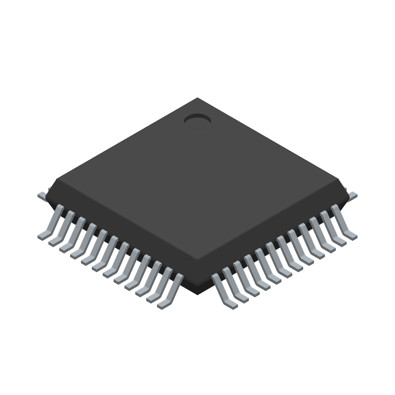
3D Model
Available Download Formats
By downloading CAD models, you agree to our Terms & Conditions and Privacy Policy

10-Bit, 40/65/80/105 MSPS 3 V Dual A/D Converter
Tip: Data for a part may vary between manufacturers. You can filter for manufacturers on the top of the page next to the part image and part number.
AD9218BST-RL105 by Analog Devices Inc is an Analog to Digital Converter.
Analog to Digital Converters are under the broader part category of Converters.
A converter is an electrical circuit that transforms electric energy into a different form that will support a elecrical load needed by a device. Read more about Converters on our Converters part category page.
| Part # | Distributor | Description | Stock | Price | Buy | |
|---|---|---|---|---|---|---|
|
|
Rochester Electronics | ADC, Proprietary Method, 10-Bit, 1 Func, 2 Channel, Parallel, Word Access, CMOS, PQFP48 RoHS: Not Compliant Status: Obsolete Min Qty: 1 | 5276 |
|
$22.7200 / $28.4000 | Buy Now |
By downloading CAD models, you agree to our Terms & Conditions and Privacy Policy
|
|
AD9218BST-RL105
Analog Devices Inc
Buy Now
Datasheet
|
Compare Parts:
AD9218BST-RL105
Analog Devices Inc
10-Bit, 40/65/80/105 MSPS 3 V Dual A/D Converter
|
| Pbfree Code | No | |
| Rohs Code | No | |
| Part Life Cycle Code | Obsolete | |
| Ihs Manufacturer | ANALOG DEVICES INC | |
| Part Package Code | QFP | |
| Package Description | 7 X 7 MM, MS-026BBC, LQFP-48 | |
| Pin Count | 48 | |
| Manufacturer Package Code | ST-48 | |
| Reach Compliance Code | not_compliant | |
| ECCN Code | EAR99 | |
| HTS Code | 8542.39.00.01 | |
| Samacsys Manufacturer | Analog Devices | |
| Analog Input Voltage-Max | 1 V | |
| Converter Type | ADC, PROPRIETARY METHOD | |
| JESD-30 Code | S-PQFP-G48 | |
| JESD-609 Code | e0 | |
| Length | 7 mm | |
| Linearity Error-Max (EL) | 0.2637% | |
| Moisture Sensitivity Level | 3 | |
| Number of Analog In Channels | 2 | |
| Number of Bits | 10 | |
| Number of Functions | 1 | |
| Number of Terminals | 48 | |
| Operating Temperature-Max | 85 °C | |
| Operating Temperature-Min | -40 °C | |
| Output Bit Code | OFFSET BINARY, 2'S COMPLEMENT BINARY | |
| Output Format | PARALLEL, WORD | |
| Package Body Material | PLASTIC/EPOXY | |
| Package Code | LFQFP | |
| Package Equivalence Code | QFP48,.35SQ,20 | |
| Package Shape | SQUARE | |
| Package Style | FLATPACK, LOW PROFILE, FINE PITCH | |
| Peak Reflow Temperature (Cel) | 240 | |
| Qualification Status | Not Qualified | |
| Sample Rate | 105 MHz | |
| Sample and Hold / Track and Hold | TRACK | |
| Seated Height-Max | 1.6 mm | |
| Supply Voltage-Nom | 3 V | |
| Surface Mount | YES | |
| Technology | CMOS | |
| Temperature Grade | INDUSTRIAL | |
| Terminal Finish | Tin/Lead (Sn85Pb15) | |
| Terminal Form | GULL WING | |
| Terminal Pitch | 0.5 mm | |
| Terminal Position | QUAD | |
| Time@Peak Reflow Temperature-Max (s) | 20 | |
| Width | 7 mm |
This table gives cross-reference parts and alternative options found for AD9218BST-RL105. The Form Fit Function (FFF) tab will give you the options that are more likely to serve as direct pin-to-pin alternates or drop-in parts. The Functional Equivalents tab will give you options that are likely to match the same function of AD9218BST-RL105, but it may not fit your design. Always verify details of parts you are evaluating, as these parts are offered as suggestions for what you are looking for and are not guaranteed.
| Part Number | Manufacturer | Composite Price | Description | Compare |
|---|---|---|---|---|
| AD9218BST-105 | Analog Devices Inc | Check for Price | 10-Bit, 40/65/80/105 MSPS 3 V Dual A/D Converter | AD9218BST-RL105 vs AD9218BST-105 |
| AD9218BSTZ-RL105 | Analog Devices Inc | Check for Price | 10-Bit, 40/65/80/105 MSPS 3 V Dual A/D Converter | AD9218BST-RL105 vs AD9218BSTZ-RL105 |
A good PCB layout is crucial for the AD9218BST-RL105. It's recommended to follow the layout guidelines provided in the datasheet, including keeping the analog and digital grounds separate, using a solid ground plane, and minimizing signal trace lengths and loops. Additionally, it's recommended to use a 4-layer PCB with a dedicated power plane and a dedicated ground plane.
To optimize the clock input, it's recommended to use a low-jitter clock source, such as a crystal oscillator or a high-quality clock generator. The clock signal should be routed as a differential pair, and the clock input pins should be terminated with a 100 ohm differential resistor. Additionally, the clock frequency should be set to the recommended range of 500 MHz to 1.2 GHz.
The maximum input signal amplitude that the AD9218BST-RL105 can handle is 1.5 Vpp differential. Exceeding this amplitude can result in signal distortion and reduced converter performance. It's recommended to use an input signal amplitude of 1.0 Vpp differential or less to ensure optimal performance.
The AD9218BST-RL105 has an internal calibration circuit that can be used to optimize its performance. The calibration process involves applying a specific calibration sequence to the device, which can be done using the SPI interface. The calibration sequence is described in the datasheet, and it's recommended to follow the calibration procedure carefully to ensure optimal performance.
The power consumption of the AD9218BST-RL105 depends on the operating frequency and the power-down mode. In normal operation, the power consumption is typically around 1.2 W. To reduce power consumption, the device can be put into a power-down mode, which reduces the power consumption to around 10 mW. Additionally, the power consumption can be reduced by reducing the operating frequency or by using a lower supply voltage.