-
Part Symbol
-
Footprint
-
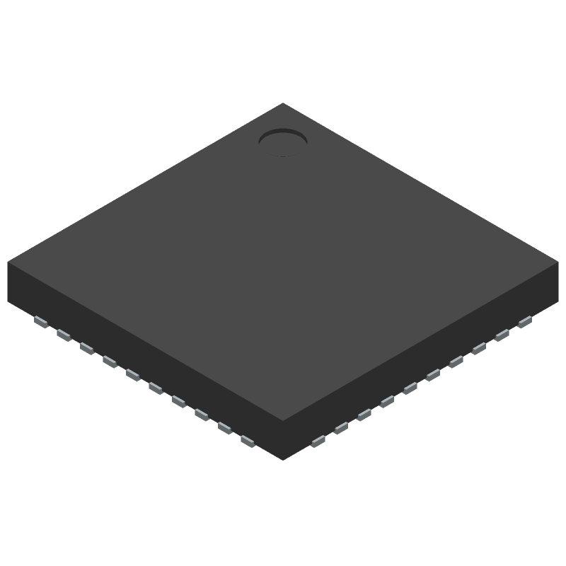
3D Model
Available Download Formats
By downloading CAD models, you agree to our Terms & Conditions and Privacy Policy
Dual Low Power, 14-Bit TxDAC Digital-to-Analog Converters
Tip: Data for a part may vary between manufacturers. You can filter for manufacturers on the top of the page next to the part image and part number.
AD9117BCPZNRL7 by Analog Devices Inc is a Digital to Analog Converter.
Digital to Analog Converters are under the broader part category of Converters.
A converter is an electrical circuit that transforms electric energy into a different form that will support a elecrical load needed by a device. Read more about Converters on our Converters part category page.
| Part # | Distributor | Description | Stock | Price | Buy | |
|---|---|---|---|---|---|---|
|
DISTI #
AD9117BCPZNRL7TR-ND
|
DigiKey | IC DAC 14BIT A-OUT 40LFCSP Min Qty: 750 Lead time: 10 Weeks Container: Tape & Reel (TR) | Temporarily Out of Stock |
|
$16.9250 | Buy Now |
|
DISTI #
584-AD9117BCPZNR7
|
Mouser Electronics | Digital to Analog Converters - DAC Dual 14B, Low Power D-A Converter RoHS: Compliant | 0 |
|
$16.9200 | Order Now |
|
|
Analog Devices Inc | Dual 14B, Low Power D-A Conver Min Qty: 750 Package Multiple: 750 | 3000 |
|
$12.5700 / $29.3500 | Buy Now |
|
DISTI #
26654200
|
Verical | DAC 2-CH Segment 14-bit 40-Pin LFCSP EP T/R RoHS: Compliant Min Qty: 750 Package Multiple: 750 | Americas - 3000 |
|
$17.0314 | Buy Now |
|
|
Vyrian | Converters | 3404 |
|
RFQ |
By downloading CAD models, you agree to our Terms & Conditions and Privacy Policy
|
|
AD9117BCPZNRL7
Analog Devices Inc
Buy Now
Datasheet
|
Compare Parts:
AD9117BCPZNRL7
Analog Devices Inc
Dual Low Power, 14-Bit TxDAC Digital-to-Analog Converters
|
| Pbfree Code | No | |
| Rohs Code | Yes | |
| Part Life Cycle Code | Active | |
| Ihs Manufacturer | ANALOG DEVICES INC | |
| Package Description | LFCSP-40 | |
| Pin Count | 40 | |
| Manufacturer Package Code | CP-40-9 | |
| Reach Compliance Code | compliant | |
| ECCN Code | EAR99 | |
| HTS Code | 8542.39.00.01 | |
| Samacsys Manufacturer | Analog Devices | |
| Analog Output Voltage-Max | 1.5 V | |
| Analog Output Voltage-Min | 0.8 V | |
| Converter Type | D/A CONVERTER | |
| Input Bit Code | BINARY, 2'S COMPLEMENT BINARY | |
| Input Format | SERIAL | |
| JESD-30 Code | S-XQCC-N40 | |
| JESD-609 Code | e4 | |
| Length | 6 mm | |
| Linearity Error-Max (EL) | 0.011% | |
| Moisture Sensitivity Level | 3 | |
| Number of Bits | 14 | |
| Number of Functions | 1 | |
| Number of Terminals | 40 | |
| Operating Temperature-Max | 85 °C | |
| Operating Temperature-Min | -40 °C | |
| Package Body Material | UNSPECIFIED | |
| Package Code | HVQCCN | |
| Package Equivalence Code | LCC40,.24SQ,20 | |
| Package Shape | SQUARE | |
| Package Style | CHIP CARRIER, HEAT SINK/SLUG, VERY THIN PROFILE | |
| Peak Reflow Temperature (Cel) | 260 | |
| Seated Height-Max | 0.8 mm | |
| Settling Time-Nom (tstl) | 0.0115 µs | |
| Supply Voltage-Nom | 1.8 V | |
| Surface Mount | YES | |
| Temperature Grade | INDUSTRIAL | |
| Terminal Finish | Nickel/Palladium/Gold (Ni/Pd/Au) | |
| Terminal Form | NO LEAD | |
| Terminal Pitch | 0.5 mm | |
| Terminal Position | QUAD | |
| Time@Peak Reflow Temperature-Max (s) | 30 | |
| Width | 6 mm |
A 4-layer PCB with a solid ground plane and a separate analog and digital power plane is recommended. Keep the analog and digital sections separate and use a star-grounding scheme to minimize noise.
The AD9117 has an internal calibration mechanism. However, it's recommended to perform an external calibration using an external reference voltage and a calibration signal to ensure optimal performance.
The maximum clock frequency is 100 MHz, but it's recommended to use a clock frequency between 10 MHz to 50 MHz for optimal performance.
The POR and BOR signals should be connected to a reset controller or a microcontroller to ensure proper system reset and initialization.
Use a combination of ceramic and electrolytic capacitors to decouple the power supply. A 10 uF ceramic capacitor and a 10 uF electrolytic capacitor in parallel is a good starting point.