-
Part Symbol
-
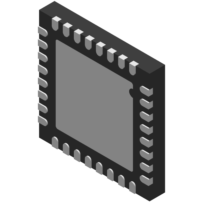
Footprint
-
3D Model
Available Download Formats
By downloading CAD models, you agree to our Terms & Conditions and Privacy Policy

41 dB Range, 1 dB Step Size, Programmable Dual VGA
Tip: Data for a part may vary between manufacturers. You can filter for manufacturers on the top of the page next to the part image and part number.
AD8372ACPZ-R7 by Analog Devices Inc is an Other Signal Circuit.
Other Signal Circuits are under the broader part category of Signal Circuits.
A signal is an electronic means of transmitting information, either as an analog signal with continuous values or a digital signal with discrete values. Signals are used in various systems and networks. Read more about Signal Circuits on our Signal Circuits part category page.
| Part # | Distributor | Description | Stock | Price | Buy | |
|---|---|---|---|---|---|---|
|
DISTI #
AD8372ACPZ-R7CT-ND
|
DigiKey | IC OPAMP VGA 2 CIRCUIT 32LFCSP Min Qty: 1 Lead time: 10 Weeks Container: Digi-Reel®, Cut Tape (CT), Tape & Reel (TR) |
1500 In Stock |
|
$11.1250 / $19.5500 | Buy Now |
|
DISTI #
584-AD8372ACPZ-R7
|
Mouser Electronics | Video Amplifiers Dual VGA for Cisco RoHS: Compliant | 372 |
|
$11.1000 / $18.9500 | Buy Now |
|
DISTI #
V72:2272_06214604
|
Arrow Electronics | SP Amp Variable Gain Amp Dual 5.5V 32-Pin LFCSP EP T/R RoHS: Compliant Min Qty: 1 Package Multiple: 1 Lead time: 10 Weeks Date Code: 1942 Container: Cut Strips | Americas - 2503 |
|
$4.6230 / $5.0950 | Buy Now |
|
|
Analog Devices Inc | Dual VGA for Cisco Min Qty: 1500 Package Multiple: 1500 | 1800 |
|
$8.4500 / $19.5500 | Buy Now |
|
DISTI #
35842678
|
Verical | SP Amp Variable Gain Amp Dual 5.5V 32-Pin LFCSP EP T/R RoHS: Compliant Min Qty: 2 Package Multiple: 1 Date Code: 1942 | Americas - 2503 |
|
$4.6230 / $5.0950 | Buy Now |
|
DISTI #
26634316
|
Verical | SP Amp Variable Gain Amp Dual 5.5V 32-Pin LFCSP EP T/R RoHS: Compliant Min Qty: 1500 Package Multiple: 1500 | Americas - 1500 |
|
$11.1950 | Buy Now |
|
|
Rochester Electronics | Analog Circuit, BICMOS RoHS: Compliant Status: Active Min Qty: 1 | 2749 |
|
$9.3400 / $11.6800 | Buy Now |
By downloading CAD models, you agree to our Terms & Conditions and Privacy Policy
|
|
AD8372ACPZ-R7
Analog Devices Inc
Buy Now
Datasheet
|
Compare Parts:
AD8372ACPZ-R7
Analog Devices Inc
41 dB Range, 1 dB Step Size, Programmable Dual VGA
|
| Pbfree Code | No | |
| Rohs Code | Yes | |
| Part Life Cycle Code | Active | |
| Ihs Manufacturer | ANALOG DEVICES INC | |
| Part Package Code | QFN | |
| Package Description | LFCSP-32 | |
| Pin Count | 32 | |
| Manufacturer Package Code | CP-32-7 | |
| Reach Compliance Code | compliant | |
| HTS Code | 8542.39.00.01 | |
| Samacsys Manufacturer | Analog Devices | |
| Analog IC - Other Type | ANALOG CIRCUIT | |
| JESD-30 Code | S-XQCC-N32 | |
| JESD-609 Code | e3 | |
| Length | 5 mm | |
| Moisture Sensitivity Level | 3 | |
| Number of Functions | 1 | |
| Number of Terminals | 32 | |
| Operating Temperature-Max | 85 °C | |
| Operating Temperature-Min | -40 °C | |
| Package Body Material | UNSPECIFIED | |
| Package Code | HVQCCN | |
| Package Equivalence Code | LCC32,.2SQ,20 | |
| Package Shape | SQUARE | |
| Package Style | CHIP CARRIER, HEAT SINK/SLUG, VERY THIN PROFILE | |
| Peak Reflow Temperature (Cel) | 260 | |
| Qualification Status | Not Qualified | |
| Seated Height-Max | 1 mm | |
| Supply Current-Max (Isup) | 270 mA | |
| Supply Voltage-Max (Vsup) | 5.5 V | |
| Supply Voltage-Min (Vsup) | 4.5 V | |
| Supply Voltage-Nom (Vsup) | 5 V | |
| Surface Mount | YES | |
| Technology | BICMOS | |
| Temperature Grade | INDUSTRIAL | |
| Terminal Finish | Matte Tin (Sn) | |
| Terminal Form | NO LEAD | |
| Terminal Pitch | 0.5 mm | |
| Terminal Position | QUAD | |
| Time@Peak Reflow Temperature-Max (s) | 30 | |
| Width | 5 mm |
This table gives cross-reference parts and alternative options found for AD8372ACPZ-R7. The Form Fit Function (FFF) tab will give you the options that are more likely to serve as direct pin-to-pin alternates or drop-in parts. The Functional Equivalents tab will give you options that are likely to match the same function of AD8372ACPZ-R7, but it may not fit your design. Always verify details of parts you are evaluating, as these parts are offered as suggestions for what you are looking for and are not guaranteed.
| Part Number | Manufacturer | Composite Price | Description | Compare |
|---|---|---|---|---|
| AD8372ACPZ-WP | Analog Devices Inc | Check for Price | 41 dB Range, 1 dB Step Size, Programmable Dual VGA | AD8372ACPZ-R7 vs AD8372ACPZ-WP |
A 4-layer PCB with a solid ground plane and a separate analog ground plane is recommended. Keep the analog and digital grounds separate and connect them at a single point. Use a star topology for the power supply connections and keep the signal traces short and direct.
Use the AD8372's internal gain and offset adjustment pins (GAIN and OFFSET) to adjust the gain and offset to suit your application. You can also use external resistors to adjust the gain and offset. Refer to the datasheet for the recommended values and equations.
Power up the device in the following sequence: AVDD, DVDD, and then the analog input signal. Ensure that the power supplies are stable and within the recommended voltage range before applying the analog input signal.
Use a shielded enclosure, keep the device away from high-frequency sources, and use a common-mode choke or ferrite bead on the analog input lines. Ensure that the PCB layout is optimized for EMC and EMI reduction.
The recommended operating temperature range is -40°C to +125°C. The device's performance may degrade at extreme temperatures, with increased noise and reduced accuracy. Ensure that the device is operated within the recommended temperature range for optimal performance.