-
Part Symbol
-
Footprint
-
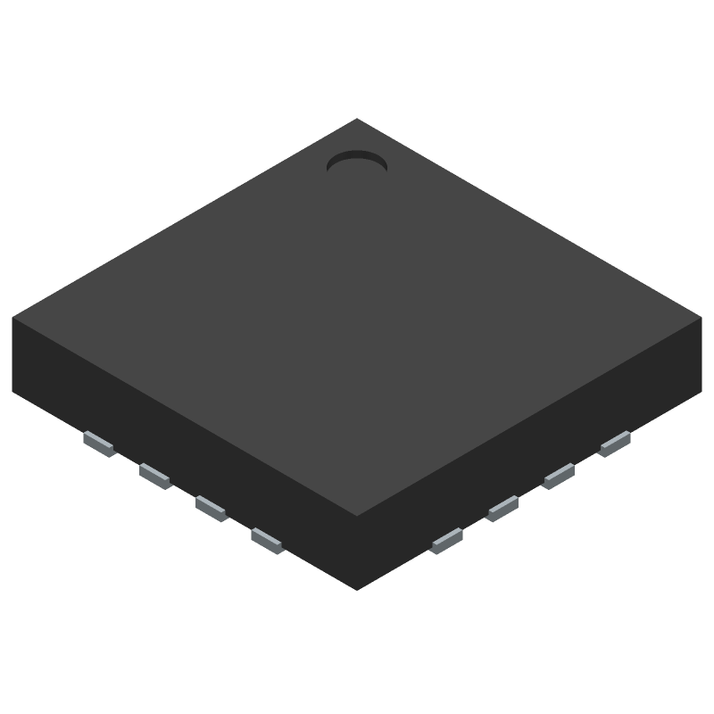
3D Model
Available Download Formats
By downloading CAD models, you agree to our Terms & Conditions and Privacy Policy
1 MHz TO 8 GHz, 70 dB Logarithmic Detector/Controller
Tip: Data for a part may vary between manufacturers. You can filter for manufacturers on the top of the page next to the part image and part number.
AD8318SCPZ-EP-R2 by Analog Devices Inc is an Analog Computational Function.
Analog Computational Functions are under the broader part category of Signal Circuits.
A signal is an electronic means of transmitting information, either as an analog signal with continuous values or a digital signal with discrete values. Signals are used in various systems and networks. Read more about Signal Circuits on our Signal Circuits part category page.
| Part # | Distributor | Description | Stock | Price | Buy | |
|---|---|---|---|---|---|---|
|
|
Analog Devices Inc | 6GHz Logarithmic Amplifier Min Qty: 250 Package Multiple: 250 | 1250 |
|
$12.3000 | Buy Now |
|
|
Vyrian | Other Function Semiconductors | 219 |
|
RFQ |
By downloading CAD models, you agree to our Terms & Conditions and Privacy Policy
|
|
AD8318SCPZ-EP-R2
Analog Devices Inc
Buy Now
Datasheet
|
Compare Parts:
AD8318SCPZ-EP-R2
Analog Devices Inc
1 MHz TO 8 GHz, 70 dB Logarithmic Detector/Controller
|
| Pbfree Code | No | |
| Rohs Code | Yes | |
| Part Life Cycle Code | Active | |
| Ihs Manufacturer | ANALOG DEVICES INC | |
| Package Description | QCCN, LCC16,.16SQ,25 | |
| Pin Count | 16 | |
| Manufacturer Package Code | CP-16-17 | |
| Reach Compliance Code | compliant | |
| ECCN Code | EAR99 | |
| HTS Code | 8542.33.00.01 | |
| Samacsys Manufacturer | Analog Devices | |
| Analog IC - Other Type | LOG OR ANTILOG AMPLIFIER | |
| Bandwidth-Nom | 7999 MHz | |
| JESD-30 Code | S-PQCC-N16 | |
| JESD-609 Code | e4 | |
| Moisture Sensitivity Level | 3 | |
| Number of Functions | 1 | |
| Number of Terminals | 16 | |
| Operating Temperature-Max | 105 °C | |
| Operating Temperature-Min | -55 °C | |
| Package Body Material | PLASTIC/EPOXY | |
| Package Code | QCCN | |
| Package Equivalence Code | LCC16,.16SQ,25 | |
| Package Shape | SQUARE | |
| Package Style | CHIP CARRIER | |
| Peak Reflow Temperature (Cel) | 260 | |
| Positive Input Voltage-Max | 3.2 V | |
| Supply Voltage-Max (Vsup) | 5.5 V | |
| Supply Voltage-Min (Vsup) | 4.5 V | |
| Supply Voltage-Nom (Vsup) | 5 V | |
| Surface Mount | YES | |
| Technology | BIPOLAR | |
| Temperature Grade | OTHER | |
| Terminal Finish | Nickel/Palladium/Gold (Ni/Pd/Au) | |
| Terminal Form | NO LEAD | |
| Terminal Pitch | 0.635 mm | |
| Terminal Position | QUAD | |
| Time@Peak Reflow Temperature-Max (s) | 30 |
A good PCB layout for the AD8318 involves keeping the input and output traces short and away from each other, using a solid ground plane, and placing decoupling capacitors close to the device. A 4-layer PCB with a dedicated ground plane is recommended. Additionally, the datasheet provides a recommended PCB layout and land pattern that should be followed.
The input termination resistor (RIN) value depends on the source impedance and the desired input impedance of the AD8318. A good starting point is to choose RIN to match the source impedance. The datasheet provides a formula to calculate RIN based on the desired input impedance and the internal impedance of the AD8318.
The maximum power that can be dissipated by the AD8318 is dependent on the ambient temperature and the thermal resistance of the package. The datasheet provides a thermal resistance value (θJA) of 45°C/W for the SCPZ package. Using this value, the maximum power dissipation can be calculated based on the ambient temperature and the desired junction temperature.
The AD8318 operates within its linear range when the input signal is within the specified range of -15 dBm to +15 dBm. The device also has a built-in detector that can be used to monitor the input power and ensure that it is within the linear range. Additionally, the datasheet provides a graph of the detector output voltage vs. input power that can be used to determine the linear range.
The recommended voltage supply decoupling for the AD8318 involves using a 10 μF capacitor in parallel with a 100 nF capacitor, both placed close to the device. This decoupling scheme helps to filter out noise and ensure stable operation of the device.