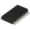
Part Details for AD7892AR-1 by Analog Devices Inc
Results Overview of AD7892AR-1 by Analog Devices Inc
- Distributor Offerings: (3 listings)
- Number of FFF Equivalents: (0 replacements)
- CAD Models: (Request Part)
- Number of Functional Equivalents: (0 options)
- Part Data Attributes: (Available)
- Reference Designs: (Not Available)
Tip: Data for a part may vary between manufacturers. You can filter for manufacturers on the top of the page next to the part image and part number.
AD7892AR-1 Information
AD7892AR-1 by Analog Devices Inc is an Analog to Digital Converter.
Analog to Digital Converters are under the broader part category of Converters.
A converter is an electrical circuit that transforms electric energy into a different form that will support a elecrical load needed by a device. Read more about Converters on our Converters part category page.
Price & Stock for AD7892AR-1
| Part # | Distributor | Description | Stock | Price | Buy | |
|---|---|---|---|---|---|---|
|
|
Quest Components | IC,A/D CONVERTER,SINGLE,12-BIT,CMOS,SOP,24PIN | 1 |
|
$47.7490 | Buy Now |
|
|
Component Electronics, Inc | IN STOCK SHIP TODAY | 7 |
|
$25.0000 / $38.4600 | Buy Now |
|
|
Vyrian | Peripheral ICs | 462 |
|
RFQ |
Part Details for AD7892AR-1
AD7892AR-1 CAD Models
AD7892AR-1 Part Data Attributes
|
|
AD7892AR-1
Analog Devices Inc
Buy Now
Datasheet
|
Compare Parts:
AD7892AR-1
Analog Devices Inc
True Bipolar Input, Single Supply, Parallel, 12-Bit 600 kSPS ADC
|
| Pbfree Code | No | |
| Rohs Code | No | |
| Part Life Cycle Code | Obsolete | |
| Ihs Manufacturer | ANALOG DEVICES INC | |
| Part Package Code | SOIC | |
| Package Description | SOIC-24 | |
| Pin Count | 24 | |
| Manufacturer Package Code | RW-24 | |
| Reach Compliance Code | not_compliant | |
| HTS Code | 8542.39.00.01 | |
| Samacsys Manufacturer | Analog Devices | |
| Analog Input Voltage-Max | 10 V | |
| Analog Input Voltage-Min | -10 V | |
| Conversion Time-Max | 1.6 µs | |
| Converter Type | ADC, SUCCESSIVE APPROXIMATION | |
| JESD-30 Code | R-PDSO-G24 | |
| JESD-609 Code | e0 | |
| Length | 15.4 mm | |
| Linearity Error-Max (EL) | 0.0366% | |
| Moisture Sensitivity Level | 1 | |
| Number of Analog In Channels | 1 | |
| Number of Bits | 12 | |
| Number of Functions | 1 | |
| Number of Terminals | 24 | |
| Operating Temperature-Max | 85 °C | |
| Operating Temperature-Min | -40 °C | |
| Output Bit Code | 2'S COMPLEMENT BINARY | |
| Output Format | SERIAL, PARALLEL, WORD | |
| Package Body Material | PLASTIC/EPOXY | |
| Package Code | SOP | |
| Package Equivalence Code | SOP24,.4 | |
| Package Shape | RECTANGULAR | |
| Package Style | SMALL OUTLINE | |
| Peak Reflow Temperature (Cel) | 240 | |
| Qualification Status | Not Qualified | |
| Sample Rate | 0.5 MHz | |
| Sample and Hold / Track and Hold | TRACK | |
| Seated Height-Max | 2.65 mm | |
| Supply Voltage-Nom | 5 V | |
| Surface Mount | YES | |
| Technology | CMOS | |
| Temperature Grade | INDUSTRIAL | |
| Terminal Finish | TIN LEAD | |
| Terminal Form | GULL WING | |
| Terminal Pitch | 1.27 mm | |
| Terminal Position | DUAL | |
| Time@Peak Reflow Temperature-Max (s) | 30 | |
| Width | 7.5 mm |
AD7892AR-1 Frequently Asked Questions (FAQ)
-
A good layout and routing practice is to keep the analog and digital grounds separate, use a star-ground configuration, and keep the analog signal traces away from the digital signal traces. Also, use a low-ESR capacitor for the VREF pin and a 0.1uF capacitor for the AVCC pin.
-
The AD7892AR-1 has an internal calibration circuit that is performed during the power-up sequence. However, it's recommended to perform an external calibration by applying a known voltage to the input and adjusting the offset and gain to achieve the desired accuracy.
-
The AD7892AR-1 has a maximum sampling rate of 250 kSPS (kilo-samples per second). However, the actual sampling rate may be limited by the system's clock frequency, the conversion time, and the settling time of the input signal.
-
The AD7892AR-1 has internal overvoltage protection up to ±16.5V. However, it's recommended to use external protection circuitry, such as voltage-limiting resistors and diodes, to prevent damage from excessive voltage levels.
-
The recommended power-up sequence is to apply the analog power supply (AVCC) first, followed by the digital power supply (DVCC), and then the clock signal. This ensures that the internal biasing and reference circuits are properly initialized.
