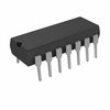
Part Details for AD7512DIJQ by Analog Devices Inc
Results Overview of AD7512DIJQ by Analog Devices Inc
- Distributor Offerings: (4 listings)
- Number of FFF Equivalents: (0 replacements)
- CAD Models: (Request Part)
- Number of Functional Equivalents: (0 options)
- Part Data Attributes: (Available)
- Reference Designs: (Not Available)
Tip: Data for a part may vary between manufacturers. You can filter for manufacturers on the top of the page next to the part image and part number.
AD7512DIJQ Information
AD7512DIJQ by Analog Devices Inc is a Multiplexer or Switch.
Multiplexers or Switches are under the broader part category of Signal Circuits.
A signal is an electronic means of transmitting information, either as an analog signal with continuous values or a digital signal with discrete values. Signals are used in various systems and networks. Read more about Signal Circuits on our Signal Circuits part category page.
Price & Stock for AD7512DIJQ
| Part # | Distributor | Description | Stock | Price | Buy | |
|---|---|---|---|---|---|---|
|
|
Quest Components | SPDT, 2 FUNC, 1 CHANNEL, CMOS, CDIP14 | 1 |
|
$90.1784 | Buy Now |
|
|
Quest Components | SPDT, 2 FUNC, 1 CHANNEL, CMOS, CDIP14 | 1 |
|
$108.2140 | Buy Now |
|
|
ComSIT USA | SPDT, 2 Func, 1 Channel, CMOS, CDIP14 RoHS: Not Compliant |
|
|
RFQ | |
|
|
Vyrian | Peripheral ICs | 1173 |
|
RFQ |
Part Details for AD7512DIJQ
AD7512DIJQ CAD Models
AD7512DIJQ Part Data Attributes
|
|
AD7512DIJQ
Analog Devices Inc
Buy Now
Datasheet
|
Compare Parts:
AD7512DIJQ
Analog Devices Inc
IC DUAL 1-CHANNEL, SGL POLE DOUBLE THROW SWITCH, CDIP14, HERMETIC SEALED, CERDIP-14, Multiplexer or Switch
|
| Pbfree Code | No | |
| Rohs Code | No | |
| Part Life Cycle Code | Obsolete | |
| Ihs Manufacturer | ANALOG DEVICES INC | |
| Part Package Code | DIP | |
| Package Description | HERMETIC SEALED, CERDIP-14 | |
| Pin Count | 14 | |
| Reach Compliance Code | not_compliant | |
| HTS Code | 8542.39.00.01 | |
| Additional Feature | OVERVOLTAGE PROTECTION | |
| Analog IC - Other Type | SPDT | |
| JESD-30 Code | R-GDIP-T14 | |
| JESD-609 Code | e0 | |
| Length | 19.43 mm | |
| Neg Supply Voltage-Nom (Vsup) | -15 V | |
| Number of Channels | 1 | |
| Number of Functions | 2 | |
| Number of Terminals | 14 | |
| On-state Resistance Match-Nom | 1 Ω | |
| On-state Resistance-Max (Ron) | 100 Ω | |
| Operating Temperature-Max | 85 °C | |
| Operating Temperature-Min | -25 °C | |
| Output | SEPARATE OUTPUT | |
| Package Body Material | CERAMIC, GLASS-SEALED | |
| Package Code | DIP | |
| Package Equivalence Code | DIP14,.3 | |
| Package Shape | RECTANGULAR | |
| Package Style | IN-LINE | |
| Qualification Status | Not Qualified | |
| Seated Height-Max | 5.08 mm | |
| Supply Current-Max (Isup) | 0.8 mA | |
| Supply Voltage-Nom (Vsup) | 15 V | |
| Surface Mount | NO | |
| Technology | CMOS | |
| Temperature Grade | OTHER | |
| Terminal Finish | TIN LEAD | |
| Terminal Form | THROUGH-HOLE | |
| Terminal Pitch | 2.54 mm | |
| Terminal Position | DUAL | |
| Width | 7.62 mm |
AD7512DIJQ Frequently Asked Questions (FAQ)
-
The AD7512DIJQ is a high-speed device, and proper layout and placement are crucial to minimize noise and ensure optimal performance. It is recommended to follow the guidelines provided in the datasheet, including keeping the analog and digital grounds separate, using a solid ground plane, and placing the device close to the analog signal sources. Additionally, it is recommended to use a 4-layer PCB with a dedicated power plane and to avoid running digital signals near the analog signals.
-
The AD7512DIJQ has a maximum junction temperature of 150°C, and proper thermal management is essential to ensure reliable operation. It is recommended to use a heat sink or a thermal pad to dissipate heat, especially in high-power applications. The thermal resistance of the package should be taken into account, and the device should be mounted on a PCB with a thermal via to dissipate heat efficiently.
-
The recommended power-up sequence for the AD7512DIJQ is to apply the analog power supply (VCC) first, followed by the digital power supply (VDD). This ensures that the analog circuitry is powered up before the digital circuitry, which helps to prevent damage or malfunction. It is also recommended to ensure that the power supplies are stable and within the recommended operating range before applying them to the device.
-
To troubleshoot issues with the AD7512DIJQ, it is recommended to follow a systematic approach, starting with the basics. Check the power supplies, clock signals, and digital communication signals to ensure they are within the recommended operating range. Use an oscilloscope to verify the output voltages and digital signals. Check the PCB layout and routing to ensure that they meet the recommended guidelines. If the issue persists, consult the datasheet and application notes for troubleshooting guides and contact Analog Devices support for further assistance.
-
The AD7512DIJQ is a sensitive device and requires proper ESD protection and handling procedures to prevent damage. It is recommended to handle the device by the body, rather than the pins, and to use an ESD wrist strap or mat when handling the device. The device should be stored in an ESD-safe environment, and ESD-sensitive devices should be separated from non-ESD-sensitive devices. Follow the recommended handling and storage procedures outlined in the datasheet and industry standards such as JEDEC JESD625-A.
