-
Part Symbol
-
Footprint
-
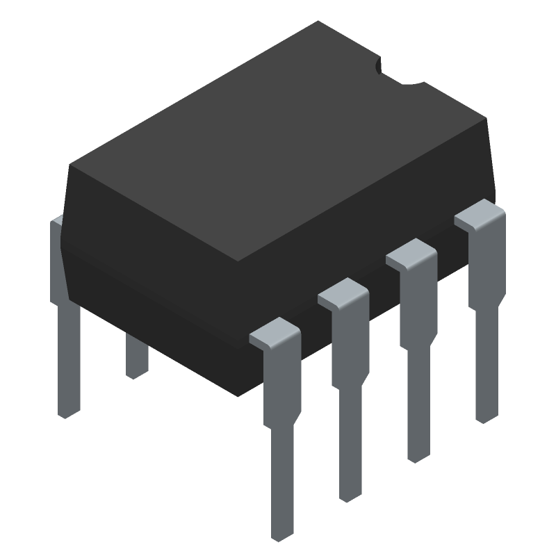
3D Model
Available Download Formats
By downloading CAD models, you agree to our Terms & Conditions and Privacy Policy

IC DUAL OP-AMP, 4000 uV OFFSET-MAX, 4 MHz BAND WIDTH, PDIP8, PLASTIC, MS-001BA, DIP-8, Operational Amplifier
Tip: Data for a part may vary between manufacturers. You can filter for manufacturers on the top of the page next to the part image and part number.
AD712JN by Analog Devices Inc is an Operational Amplifier.
Operational Amplifiers are under the broader part category of Amplifier Circuits.
Amplifier circuits use external power to increase the amplitude of an input signal. They can be used to perform linear amplifications or logarithmic functions. Read more about Amplifier Circuits on our Amplifier Circuits part category page.
| Part # | Distributor | Description | Stock | Price | Buy | |
|---|---|---|---|---|---|---|
|
|
Bristol Electronics | Min Qty: 1 | 247 |
|
$2.6863 / $6.5520 | Buy Now |
|
|
Quest Components | IC,OP-AMP,DUAL,BIPOLAR/JFET,DIP,8PIN,PLASTIC | 1517 |
|
$6.7500 / $13.5000 | Buy Now |
|
|
Quest Components | IC,OP-AMP,DUAL,BIPOLAR/JFET,DIP,8PIN,PLASTIC | 169 |
|
$3.8025 / $8.7750 | Buy Now |
|
|
Quest Components | IC,OP-AMP,DUAL,BIPOLAR/JFET,DIP,8PIN,PLASTIC | 110 |
|
$5.5500 / $9.0000 | Buy Now |
|
|
Quest Components | IC,OP-AMP,DUAL,BIPOLAR/JFET,DIP,8PIN,PLASTIC | 88 |
|
$5.9246 / $9.6075 | Buy Now |
|
|
Quest Components | IC,OP-AMP,DUAL,BIPOLAR/JFET,DIP,8PIN,PLASTIC | 60 |
|
$4.0000 / $6.0000 | Buy Now |
|
|
Quest Components | IC,OP-AMP,DUAL,BIPOLAR/JFET,DIP,8PIN,PLASTIC | 12 |
|
$2.3100 / $4.6200 | Buy Now |
|
|
Quest Components | IC,OP-AMP,DUAL,BIPOLAR/JFET,DIP,8PIN,PLASTIC | 10 |
|
$10.0000 / $15.0000 | Buy Now |
|
|
ComSIT USA | Electronic Component RoHS: Not Compliant |
|
|
RFQ | |
|
|
Vyrian | Peripheral ICs | 395 |
|
RFQ |
By downloading CAD models, you agree to our Terms & Conditions and Privacy Policy
|
|
AD712JN
Analog Devices Inc
Buy Now
Datasheet
|
Compare Parts:
AD712JN
Analog Devices Inc
IC DUAL OP-AMP, 4000 uV OFFSET-MAX, 4 MHz BAND WIDTH, PDIP8, PLASTIC, MS-001BA, DIP-8, Operational Amplifier
|
| Rohs Code | No | |
| Part Life Cycle Code | Obsolete | |
| Ihs Manufacturer | ANALOG DEVICES INC | |
| Part Package Code | DIP | |
| Package Description | PLASTIC, MS-001BA, DIP-8 | |
| Pin Count | 8 | |
| Reach Compliance Code | not_compliant | |
| ECCN Code | EAR99 | |
| HTS Code | 8542.33.00.01 | |
| Samacsys Manufacturer | Analog Devices | |
| Amplifier Type | OPERATIONAL AMPLIFIER | |
| Architecture | VOLTAGE-FEEDBACK | |
| Average Bias Current-Max (IIB) | 0.0001 µA | |
| Bias Current-Max (IIB) @25C | 0.0001 µA | |
| Common-mode Reject Ratio-Min | 70 dB | |
| Common-mode Reject Ratio-Nom | 80 dB | |
| Frequency Compensation | YES | |
| Input Offset Current-Max (IIO) | 0.0006 µA | |
| Input Offset Voltage-Max | 4000 µV | |
| JESD-30 Code | R-PDIP-T8 | |
| JESD-609 Code | e0 | |
| Length | 9.27 mm | |
| Low-Bias | YES | |
| Low-Offset | NO | |
| Neg Supply Voltage Limit-Max | -18 V | |
| Neg Supply Voltage-Nom (Vsup) | -15 V | |
| Number of Functions | 2 | |
| Number of Terminals | 8 | |
| Operating Temperature-Max | 70 °C | |
| Operating Temperature-Min | ||
| Package Body Material | PLASTIC/EPOXY | |
| Package Code | DIP | |
| Package Equivalence Code | DIP8,.3 | |
| Package Shape | RECTANGULAR | |
| Package Style | IN-LINE | |
| Peak Reflow Temperature (Cel) | 260 | |
| Qualification Status | Not Qualified | |
| Seated Height-Max | 5.33 mm | |
| Slew Rate-Min | 16 V/us | |
| Slew Rate-Nom | 20 V/us | |
| Supply Current-Max | 6.8 mA | |
| Supply Voltage Limit-Max | 18 V | |
| Supply Voltage-Nom (Vsup) | 15 V | |
| Surface Mount | NO | |
| Technology | BIPOLAR | |
| Temperature Grade | COMMERCIAL | |
| Terminal Finish | TIN LEAD | |
| Terminal Form | THROUGH-HOLE | |
| Terminal Pitch | 2.54 mm | |
| Terminal Position | DUAL | |
| Time@Peak Reflow Temperature-Max (s) | 40 | |
| Unity Gain BW-Nom | 4000 | |
| Voltage Gain-Min | 100000 | |
| Width | 7.62 mm |
The AD7124JN requires careful layout and placement to minimize noise and ensure optimal performance. It is recommended to place the device close to the analog signal sources, use a solid ground plane, and keep the analog and digital signals separate. Additionally, decoupling capacitors should be placed close to the device's power pins.
To optimize the AD7124JN's analog-to-digital conversion, it is essential to understand the device's analog input range, gain, and offset. The user should select the appropriate gain and offset settings based on the application's requirements. Additionally, the user should ensure that the analog input signal is within the device's input range and that the signal is properly filtered and buffered.
The recommended power-up sequence for the AD7124JN is to first apply the analog power supply (AVDD) and then the digital power supply (DVDD). The user should ensure that the power supplies are stable and within the recommended operating range before applying the clock signal.
To troubleshoot common issues with the AD7124JN, the user should first verify that the device is properly powered and configured. The user should then check the analog input signal and ensure that it is within the device's input range. If the issue persists, the user should check the device's digital output and verify that it is properly connected to the microcontroller or other digital device.
The AD7124JN has a maximum junction temperature of 150°C. To ensure reliable operation over temperature, the user should ensure that the device is properly heat-sinked and that the ambient temperature is within the recommended operating range. The user should also ensure that the device is not exposed to excessive thermal stress or mechanical stress.