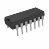
Part Details for AD637KD by Analog Devices Inc
Results Overview of AD637KD by Analog Devices Inc
- Distributor Offerings: (1 listing)
- Number of FFF Equivalents: (2 replacements)
- CAD Models: (Request Part)
- Number of Functional Equivalents: (10 options)
- Part Data Attributes: (Available)
- Reference Designs: (Not Available)
Tip: Data for a part may vary between manufacturers. You can filter for manufacturers on the top of the page next to the part image and part number.
AD637KD Information
AD637KD by Analog Devices Inc is an Analog Special Function Converter.
Analog Special Function Converters are under the broader part category of Converters.
A converter is an electrical circuit that transforms electric energy into a different form that will support a elecrical load needed by a device. Read more about Converters on our Converters part category page.
Price & Stock for AD637KD
| Part # | Distributor | Description | Stock | Price | Buy | |
|---|---|---|---|---|---|---|
|
|
Vyrian | Converters | 34 |
|
RFQ |
Part Details for AD637KD
AD637KD CAD Models
AD637KD Part Data Attributes
|
|
AD637KD
Analog Devices Inc
Buy Now
Datasheet
|
Compare Parts:
AD637KD
Analog Devices Inc
IC RMS TO DC CONVERTER, 0.15 MHz, CDIP14, SIDE BRAZED, CERAMIC, DIP-14, Analog Special Function Converter
|
| Rohs Code | No | |
| Part Life Cycle Code | Obsolete | |
| Ihs Manufacturer | ANALOG DEVICES INC | |
| Part Package Code | DIP | |
| Package Description | SIDE BRAZED, CERAMIC, DIP-14 | |
| Pin Count | 14 | |
| Reach Compliance Code | not_compliant | |
| HTS Code | 8542.39.00.01 | |
| Converter Type | RMS TO DC CONVERTER | |
| JESD-30 Code | R-CDIP-T14 | |
| JESD-609 Code | e0 | |
| Length | 19.43 mm | |
| Linearity Error-Max (EL) | 0.05% | |
| Negative Supply Voltage-Max | -18 V | |
| Negative Supply Voltage-Min | -3 V | |
| Negative Supply Voltage-Nom | -15 V | |
| Number of Functions | 1 | |
| Number of Terminals | 14 | |
| Operating Frequency-Max | 0.15 MHz | |
| Operating Temperature-Max | 70 °C | |
| Operating Temperature-Min | ||
| Package Body Material | CERAMIC, METAL-SEALED COFIRED | |
| Package Code | DIP | |
| Package Equivalence Code | DIP14,.3 | |
| Package Shape | RECTANGULAR | |
| Package Style | IN-LINE | |
| Positive Input Voltage-Max | 7 V | |
| Qualification Status | Not Qualified | |
| Seated Height-Max | 5.08 mm | |
| Supply Current-Max | 3 mA | |
| Supply Voltage-Max | 18 V | |
| Supply Voltage-Min | 3 V | |
| Supply Voltage-Nom | 15 V | |
| Surface Mount | NO | |
| Temperature Grade | COMMERCIAL | |
| Terminal Finish | TIN LEAD | |
| Terminal Form | THROUGH-HOLE | |
| Terminal Pitch | 2.54 mm | |
| Terminal Position | DUAL | |
| Total Error-Max | 0.3% | |
| Width | 7.62 mm |
Alternate Parts for AD637KD
This table gives cross-reference parts and alternative options found for AD637KD. The Form Fit Function (FFF) tab will give you the options that are more likely to serve as direct pin-to-pin alternates or drop-in parts. The Functional Equivalents tab will give you options that are likely to match the same function of AD637KD, but it may not fit your design. Always verify details of parts you are evaluating, as these parts are offered as suggestions for what you are looking for and are not guaranteed.
| Part Number | Manufacturer | Composite Price | Description | Compare |
|---|---|---|---|---|
| AD637KQ | Analog Devices Inc | Check for Price | High Precision, Wideband RMS-to-DC Converter | AD637KD vs AD637KQ |
| AD637KD/+ | Analog Devices Inc | Check for Price | IC RMS TO DC CONVERTER, 0.15 MHz, CDIP14, SIDE BRAZED, CERAMIC, DIP-14, Analog Special Function Converter | AD637KD vs AD637KD/+ |
AD637KD Frequently Asked Questions (FAQ)
-
A good PCB layout for the AD637KD involves keeping the input and output traces separate, using a ground plane, and placing decoupling capacitors close to the device. Additionally, it's recommended to use a 4-layer PCB with a dedicated power plane and a dedicated ground plane to reduce noise and electromagnetic interference (EMI).
-
To ensure the accuracy of the AD637KD's output voltage over temperature, it's essential to consider the device's temperature coefficient, which is specified in the datasheet. Additionally, using a high-precision voltage reference and a low-temperature-coefficient resistor network can help minimize temperature-related errors. It's also recommended to calibrate the device over the operating temperature range to account for any temperature-related drift.
-
The maximum allowable input voltage for the AD637KD is 36V, but it's recommended to keep the input voltage below 30V to ensure optimal performance and prevent damage to the device. Exceeding the maximum input voltage can lead to reduced accuracy, increased noise, and potentially even device failure.
-
To troubleshoot common issues with the AD637KD, start by checking the input voltage, output load, and PCB layout for any potential issues. Verify that the device is properly powered and that the input voltage is within the specified range. Check for any signs of overheating, and ensure that the device is properly decoupled. If the issue persists, consult the datasheet and application notes for guidance, or contact Analog Devices' technical support for further assistance.
-
Yes, the AD637KD can be used in high-reliability or safety-critical applications, but it's essential to follow proper design and testing procedures to ensure the device meets the required safety and reliability standards. Considerations include using a redundant design, implementing error detection and correction mechanisms, and performing thorough testing and validation to ensure the device meets the required specifications and standards.
