-
Part Symbol
-
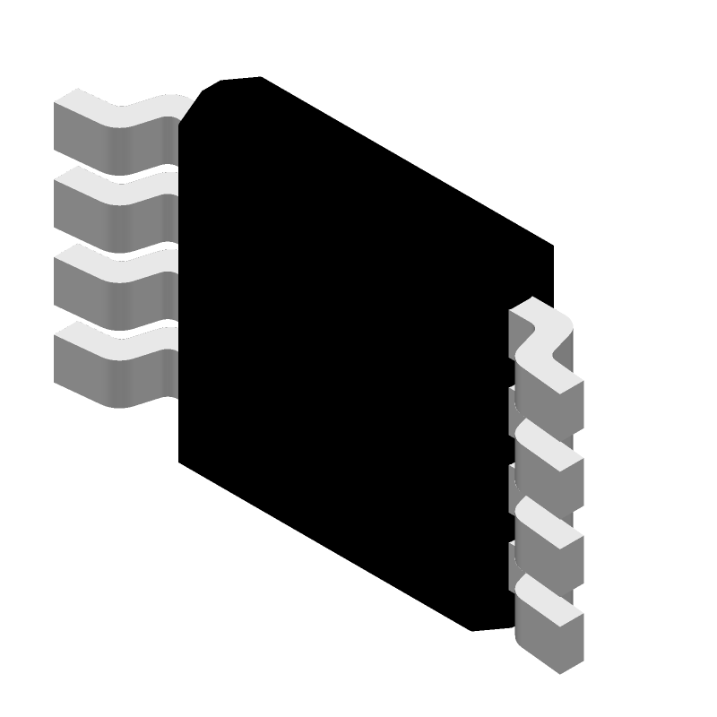
Footprint
-
3D Model
Available Download Formats
By downloading CAD models, you agree to our Terms & Conditions and Privacy Policy

2.5 V to 5.5 V, 250 µA, 2-Wire Interface, Dual Voltage Output, 10-Bit DACs
Tip: Data for a part may vary between manufacturers. You can filter for manufacturers on the top of the page next to the part image and part number.
AD5338BRMZ-1 by Analog Devices Inc is a Digital to Analog Converter.
Digital to Analog Converters are under the broader part category of Converters.
A converter is an electrical circuit that transforms electric energy into a different form that will support a elecrical load needed by a device. Read more about Converters on our Converters part category page.
| Part # | Distributor | Description | Stock | Price | Buy | |
|---|---|---|---|---|---|---|
|
|
Rochester Electronics | Dual, 10-Bit nanoDAC with Reference, I2C Interface RoHS: Compliant Status: Obsolete Min Qty: 1 | 2631 |
|
$3.0200 / $3.7800 | Buy Now |
By downloading CAD models, you agree to our Terms & Conditions and Privacy Policy
|
|
AD5338BRMZ-1
Analog Devices Inc
Buy Now
Datasheet
|
Compare Parts:
AD5338BRMZ-1
Analog Devices Inc
2.5 V to 5.5 V, 250 µA, 2-Wire Interface, Dual Voltage Output, 10-Bit DACs
|
| Pbfree Code | No | |
| Rohs Code | Yes | |
| Part Life Cycle Code | Obsolete | |
| Ihs Manufacturer | ANALOG DEVICES INC | |
| Part Package Code | TSSOP | |
| Package Description | ROHS COMPLIANT, MO-187AA, MSOP-8 | |
| Pin Count | 8 | |
| Manufacturer Package Code | RM-8 | |
| Reach Compliance Code | unknown | |
| HTS Code | 8542.39.00.01 | |
| Samacsys Manufacturer | Analog Devices | |
| Analog Output Voltage-Max | 5.499 V | |
| Analog Output Voltage-Min | 0.001 V | |
| Converter Type | D/A CONVERTER | |
| Input Bit Code | BINARY | |
| Input Format | SERIAL | |
| JESD-30 Code | S-PDSO-G8 | |
| JESD-609 Code | e3 | |
| Length | 3 mm | |
| Linearity Error-Max (EL) | 0.1953% | |
| Moisture Sensitivity Level | 1 | |
| Number of Bits | 10 | |
| Number of Functions | 1 | |
| Number of Terminals | 8 | |
| Operating Temperature-Max | 105 °C | |
| Operating Temperature-Min | -40 °C | |
| Package Body Material | PLASTIC/EPOXY | |
| Package Code | TSSOP | |
| Package Equivalence Code | TSSOP8,.19 | |
| Package Shape | SQUARE | |
| Package Style | SMALL OUTLINE, THIN PROFILE, SHRINK PITCH | |
| Peak Reflow Temperature (Cel) | 260 | |
| Qualification Status | Not Qualified | |
| Seated Height-Max | 1.1 mm | |
| Settling Time-Max | 9 µs | |
| Settling Time-Nom (tstl) | 7 µs | |
| Supply Current-Max | 0.375 mA | |
| Supply Voltage-Nom | 3 V | |
| Surface Mount | YES | |
| Technology | CMOS | |
| Temperature Grade | INDUSTRIAL | |
| Terminal Finish | Matte Tin (Sn) - annealed | |
| Terminal Form | GULL WING | |
| Terminal Pitch | 0.65 mm | |
| Terminal Position | DUAL | |
| Width | 3 mm |
A good layout and routing practice for the AD5338BRMZ-1 involves keeping the analog and digital grounds separate, using a solid ground plane, and minimizing the length of the traces connected to the output pins. Additionally, it's recommended to place the device close to the power supply and to use decoupling capacitors to filter out noise.
To ensure the accuracy and linearity of the DAC output voltage, it's essential to follow the recommended calibration procedure, use a high-quality reference voltage, and minimize the noise and interference in the system. Additionally, the output voltage should be buffered with an op-amp to prevent loading effects.
The AD5338BRMZ-1 can provide a maximum output current of 10 mA. However, it's recommended to limit the output current to 5 mA to ensure the device operates within its specified temperature range and to prevent overheating.
The AD5338BRMZ-1 can be interfaced with a microcontroller or FPGA using a serial interface such as SPI or I2C. The device requires a clock signal, a chip select signal, and data input pins. The interface protocol and timing requirements are specified in the datasheet.
The AD5338BRMZ-1 has a power-on reset feature that initializes the device to a default state when the power supply is turned on. The output voltage is set to 0 V, and the device is in a low-power state. The power-on reset behavior can be modified by using external circuitry or by programming the device's internal registers.