-
Part Symbol
-
Footprint
-
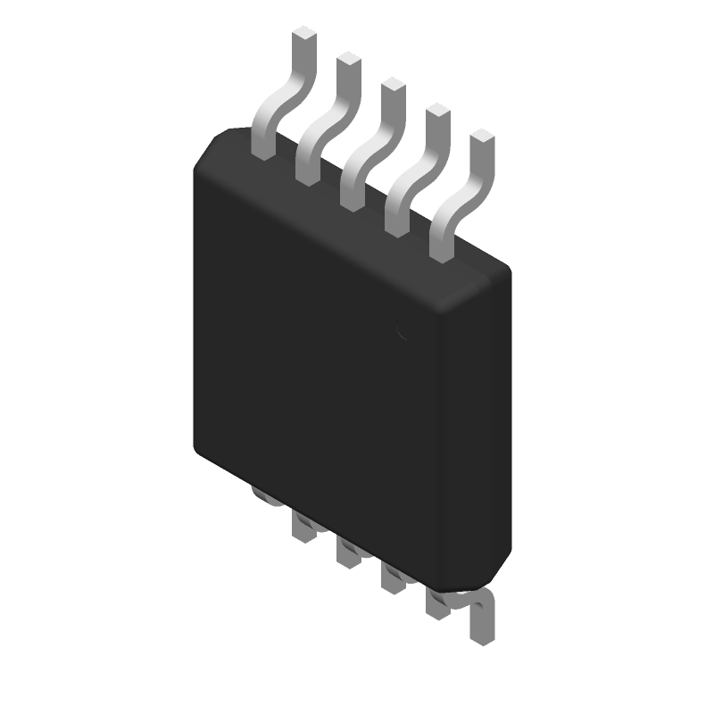
3D Model
Available Download Formats
By downloading CAD models, you agree to our Terms & Conditions and Privacy Policy

2.5 V to 5.5 V, 500 µA Quad Voltage Output 12-Bit DAC in 10-Lead Packages
Tip: Data for a part may vary between manufacturers. You can filter for manufacturers on the top of the page next to the part image and part number.
AD5324SRMZ-EP-RL7 by Analog Devices Inc is a Digital to Analog Converter.
Digital to Analog Converters are under the broader part category of Converters.
A converter is an electrical circuit that transforms electric energy into a different form that will support a elecrical load needed by a device. Read more about Converters on our Converters part category page.
| Part # | Distributor | Description | Stock | Price | Buy | |
|---|---|---|---|---|---|---|
|
DISTI #
AD5324SRMZ-EP-RL7CT-ND
|
DigiKey | IC DAC 12BIT V-OUT 10MSOP Min Qty: 1 Lead time: 20 Weeks Container: Digi-Reel®, Cut Tape (CT), Tape & Reel (TR) |
15 In Stock |
|
$18.1500 / $28.5600 | Buy Now |
|
DISTI #
584-AD5324SRMZ-EP-R7
|
Mouser Electronics | Digital to Analog Converters - DAC 12-BIT QUAD DAC I.C. RoHS: Compliant | 0 |
|
$18.7000 / $28.2000 | Order Now |
|
DISTI #
V72:2272_06207972
|
Arrow Electronics | DAC 4-CH Resistor-String 12-bit 10-Pin MSOP T/R RoHS: Compliant Min Qty: 1 Package Multiple: 1 Lead time: 10 Weeks Date Code: 1950 Container: Cut Strips | Americas - 161 |
|
$18.6200 / $23.0100 | Buy Now |
|
DISTI #
57454779
|
Verical | DAC 4-CH Resistor-String 12-bit 10-Pin MSOP T/R RoHS: Compliant Min Qty: 1 Package Multiple: 1 Date Code: 1950 | Americas - 161 |
|
$18.6200 / $23.0100 | Buy Now |
|
|
Rochester Electronics | 2.5V to 5.5V, 500uA, Quad Voltage Output 12-Bit DAC RoHS: Compliant Status: Active Min Qty: 1 | 7003 |
|
$15.2900 / $19.1100 | Buy Now |
|
DISTI #
AD5324SRMZ-EPR7
|
Richardson RFPD | CONVERTER - DAC RoHS: Compliant Min Qty: 1000 | 0 |
|
$18.9900 | Buy Now |
By downloading CAD models, you agree to our Terms & Conditions and Privacy Policy
|
|
AD5324SRMZ-EP-RL7
Analog Devices Inc
Buy Now
Datasheet
|
Compare Parts:
AD5324SRMZ-EP-RL7
Analog Devices Inc
2.5 V to 5.5 V, 500 µA Quad Voltage Output 12-Bit DAC in 10-Lead Packages
|
| Pbfree Code | No | |
| Rohs Code | Yes | |
| Part Life Cycle Code | Active | |
| Ihs Manufacturer | ANALOG DEVICES INC | |
| Part Package Code | TSSOP | |
| Package Description | MO-187BA, MSOP-10 | |
| Pin Count | 10 | |
| Manufacturer Package Code | RM-10 | |
| Reach Compliance Code | compliant | |
| ECCN Code | 3A001.A.2.C | |
| HTS Code | 8542.39.00.01 | |
| Samacsys Manufacturer | Analog Devices | |
| Analog Output Voltage-Max | 5.5 V | |
| Analog Output Voltage-Min | 0.25 V | |
| Converter Type | D/A CONVERTER | |
| Input Bit Code | BINARY | |
| Input Format | SERIAL | |
| JESD-30 Code | S-PDSO-G10 | |
| JESD-609 Code | e4 | |
| Length | 3 mm | |
| Linearity Error-Max (EL) | 0.2441% | |
| Moisture Sensitivity Level | 1 | |
| Number of Bits | 12 | |
| Number of Functions | 1 | |
| Number of Terminals | 10 | |
| Operating Temperature-Max | 125 °C | |
| Operating Temperature-Min | -55 °C | |
| Package Body Material | PLASTIC/EPOXY | |
| Package Code | TSSOP | |
| Package Shape | SQUARE | |
| Package Style | SMALL OUTLINE, THIN PROFILE, SHRINK PITCH | |
| Peak Reflow Temperature (Cel) | 260 | |
| Seated Height-Max | 1.1 mm | |
| Settling Time-Nom (tstl) | 8 µs | |
| Supply Voltage-Nom | 3 V | |
| Surface Mount | YES | |
| Temperature Grade | MILITARY | |
| Terminal Finish | Nickel/Palladium/Gold (Ni/Pd/Au) | |
| Terminal Form | GULL WING | |
| Terminal Pitch | 0.5 mm | |
| Terminal Position | DUAL | |
| Width | 3 mm |
A good PCB layout for the AD5324SRMZ-EP-RL7 involves keeping the analog and digital grounds separate, using a solid ground plane, and minimizing noise coupling between the analog and digital sections. A 4-layer PCB with a dedicated analog ground plane is recommended.
To ensure accurate voltage reference performance, it's essential to decouple the VREF pin with a 10uF capacitor to GND, and use a low-noise, low-impedance voltage source for the VCC pin. Additionally, keep the voltage reference input pin (VIN) away from noisy digital signals.
The recommended power-up sequence is to apply VCC first, followed by the voltage reference input (VIN). This ensures that the internal voltage regulator is powered up before the analog circuitry.
To minimize digital noise coupling, use a separate analog ground plane, keep digital signals away from the analog section, and use shielding or guard rings around the analog signals. Additionally, use a low-noise, low-impedance voltage source for the VCC pin.
The maximum allowed capacitance on the VOUT pin is 10nF. Exceeding this value may cause instability or oscillations in the output stage.