-
Part Symbol
-
Footprint
-
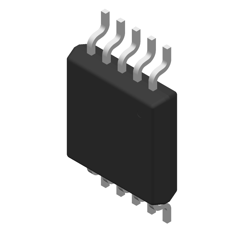
3D Model
Available Download Formats
By downloading CAD models, you agree to our Terms & Conditions and Privacy Policy

2.5 V to 5.5 V, 230 µA, Dual Rail-to-Rail Voltage Output 10-Bit DAC
Tip: Data for a part may vary between manufacturers. You can filter for manufacturers on the top of the page next to the part image and part number.
AD5312BRMZ by Analog Devices Inc is a Digital to Analog Converter.
Digital to Analog Converters are under the broader part category of Converters.
A converter is an electrical circuit that transforms electric energy into a different form that will support a elecrical load needed by a device. Read more about Converters on our Converters part category page.
| Part # | Distributor | Description | Stock | Price | Buy | |
|---|---|---|---|---|---|---|
|
DISTI #
60AK6403
|
Newark | Dac, 10Bit, Msop-10, -40 To 105Deg C, Resolution (Bits):10Bit, Sampling Rate:-, Data Interface:3 Wire, Microwire, Qspi, Serial, Spi, Supply Voltage Range:2.5V To 5.5V, Adc/Dac Case Style:Msop, No. Of Pins:10Pins Rohs Compliant: Yes |Analog Devices AD5312BRMZ RoHS: Compliant Min Qty: 1 Package Multiple: 1 Date Code: 1 Container: Bulk | 84 |
|
$5.5700 / $9.6300 | Buy Now |
|
DISTI #
AD5312BRMZ-ND
|
DigiKey | IC DAC 10BIT V-OUT 10MSOP Min Qty: 1 Lead time: 10 Weeks Container: Tube |
162 In Stock |
|
$5.2875 / $11.1300 | Buy Now |
|
DISTI #
584-AD5312BRMZ
|
Mouser Electronics | Digital to Analog Converters - DAC DUAL 10-BIT VOLTAGE OUT DAC I.C. RoHS: Compliant | 201 |
|
$5.2800 / $10.3000 | Buy Now |
|
|
Analog Devices Inc | DUAL 10-BIT VOLTAGE OUT DAC I. Package Multiple: 50 | 83 |
|
$3.7700 / $11.1300 | Buy Now |
|
DISTI #
26615704
|
Verical | DAC 2-CH Resistor-String 10-bit 10-Pin MSOP Tube RoHS: Compliant Min Qty: 100 Package Multiple: 100 | Americas - 100 |
|
$5.2319 | Buy Now |
|
DISTI #
77832838
|
Verical | DAC 2-CH Resistor-String 10-bit 10-Pin MSOP Tube RoHS: Compliant Min Qty: 20 Package Multiple: 20 Date Code: 2302 | Americas - 20 |
|
$11.4288 | Buy Now |
|
|
Bristol Electronics | 6 |
|
RFQ | ||
|
|
Quest Components | 1 |
|
$10.3557 | Buy Now | |
|
DISTI #
AD5312BRMZ
|
TME | IC: D/A converter, 10bit, Ch: 2, 2.5÷5.5V, MSOP10, -40÷105°C Min Qty: 1 | 0 |
|
$5.5100 / $7.7100 | RFQ |
|
|
ComSIT USA | 2.5 V TO 5.5 V, 230 MICROAMP, DUAL RAIL-TO-RAIL, VOLTAGE OUTPUT 10-BIT DAC D/A Converter, 1 Func, Serial Input Loading, 7us Settling Time, PDSO10 ECCN: EAR99 RoHS: Compliant |
|
|
RFQ |
By downloading CAD models, you agree to our Terms & Conditions and Privacy Policy
|
|
AD5312BRMZ
Analog Devices Inc
Buy Now
Datasheet
|
Compare Parts:
AD5312BRMZ
Analog Devices Inc
2.5 V to 5.5 V, 230 µA, Dual Rail-to-Rail Voltage Output 10-Bit DAC
|
| Pbfree Code | No | |
| Rohs Code | Yes | |
| Part Life Cycle Code | Active | |
| Ihs Manufacturer | ANALOG DEVICES INC | |
| Part Package Code | TSSOP | |
| Package Description | ROHS COMPLIANT, MO-187BA, MSOP-10 | |
| Pin Count | 10 | |
| Manufacturer Package Code | RM-10 | |
| Reach Compliance Code | compliant | |
| ECCN Code | EAR99 | |
| HTS Code | 8542.39.00.01 | |
| Samacsys Manufacturer | Analog Devices | |
| Analog Output Voltage-Max | 5.499 V | |
| Analog Output Voltage-Min | 0.001 V | |
| Converter Type | D/A CONVERTER | |
| Input Bit Code | BINARY | |
| Input Format | SERIAL | |
| JESD-30 Code | S-PDSO-G10 | |
| JESD-609 Code | e3 | |
| Length | 3 mm | |
| Linearity Error-Max (EL) | 0.1953% | |
| Moisture Sensitivity Level | 1 | |
| Number of Bits | 10 | |
| Number of Functions | 1 | |
| Number of Terminals | 10 | |
| Operating Temperature-Max | 105 °C | |
| Operating Temperature-Min | -40 °C | |
| Package Body Material | PLASTIC/EPOXY | |
| Package Code | TSSOP | |
| Package Equivalence Code | TSSOP10,.19,20 | |
| Package Shape | SQUARE | |
| Package Style | SMALL OUTLINE, THIN PROFILE, SHRINK PITCH | |
| Peak Reflow Temperature (Cel) | 260 | |
| Qualification Status | Not Qualified | |
| Seated Height-Max | 1.1 mm | |
| Settling Time-Max | 9 µs | |
| Settling Time-Nom (tstl) | 7 µs | |
| Supply Current-Max | 0.45 mA | |
| Supply Voltage-Nom | 3 V | |
| Surface Mount | YES | |
| Technology | CMOS | |
| Temperature Grade | INDUSTRIAL | |
| Terminal Finish | Matte Tin (Sn) | |
| Terminal Form | GULL WING | |
| Terminal Pitch | 0.5 mm | |
| Terminal Position | DUAL | |
| Time@Peak Reflow Temperature-Max (s) | 30 | |
| Width | 3 mm |
This table gives cross-reference parts and alternative options found for AD5312BRMZ. The Form Fit Function (FFF) tab will give you the options that are more likely to serve as direct pin-to-pin alternates or drop-in parts. The Functional Equivalents tab will give you options that are likely to match the same function of AD5312BRMZ, but it may not fit your design. Always verify details of parts you are evaluating, as these parts are offered as suggestions for what you are looking for and are not guaranteed.
| Part Number | Manufacturer | Composite Price | Description | Compare |
|---|---|---|---|---|
| AD5312BRMZ-REEL7 | Analog Devices Inc | $6.2557 | 2.5 V to 5.5 V, 230 µA, Dual Rail-to-Rail Voltage Output 10-Bit DAC | AD5312BRMZ vs AD5312BRMZ-REEL7 |
| AD5312BRM-REEL | Analog Devices Inc | Check for Price | IC SERIAL INPUT LOADING, 7 us SETTLING TIME, 10-BIT DAC, PDSO10, MO-187BA, MSOP-10, Digital to Analog Converter | AD5312BRMZ vs AD5312BRM-REEL |
| AD5312BRM-REEL7 | Analog Devices Inc | Check for Price | 2.5 V to 5.5 V, 230 µA, Dual Rail-to-Rail Voltage Output 10-Bit DAC | AD5312BRMZ vs AD5312BRM-REEL7 |
It is recommended to follow a star-grounding scheme, keeping the analog and digital grounds separate, and placing the device close to the analog signal sources. Additionally, ensure that the device is placed away from high-frequency noise sources and that the PCB layout is designed to minimize electromagnetic interference (EMI).
To ensure accurate voltage reference performance, it is recommended to use a high-quality external capacitor (e.g., 10uF) connected between the VREF and GND pins. Additionally, consider using a voltage reference with a low temperature coefficient (e.g., AD581 or AD587) and ensure that the device is operated within its specified temperature range.
The recommended power-up sequence is to first apply the analog supply voltage (VCC) and then the digital supply voltage (VDD). Ensure that the power supplies are stable and within the specified voltage range before applying the input signals.
The internal voltage reference requires a startup time of approximately 10ms. To ensure proper initialization, wait for at least 10ms after power-up before applying input signals or starting conversions. You can also use the /RESET pin to reset the device and restart the internal voltage reference.
It is recommended to use a low-pass filter (e.g., RC filter) to remove high-frequency noise from the input signals. Additionally, consider using a buffer amplifier or an instrumentation amplifier to condition the input signals and ensure that they are within the specified input range.