-
Part Symbol
-
Footprint
-
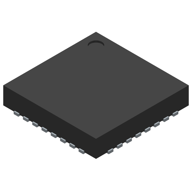
3D Model
Available Download Formats
By downloading CAD models, you agree to our Terms & Conditions and Privacy Policy

Power Supply Support Circuit, Adjustable, 7 Channel, TQFN-32
Tip: Data for a part may vary between manufacturers. You can filter for manufacturers on the top of the page next to the part image and part number.
ACT8865QI405-T by Active-Semi is a Power Management Circuit.
Power Management Circuits are under the broader part category of Power Circuits.
A power circuit delivers electricity in order to operate a load for an electronic device. Power circuits include transformers, generators and switches. Read more about Power Circuits on our Power Circuits part category page.
By downloading CAD models, you agree to our Terms & Conditions and Privacy Policy
|
|
ACT8865QI405-T
Active-Semi
Buy Now
Datasheet
|
Compare Parts:
ACT8865QI405-T
Active-Semi
Power Supply Support Circuit, Adjustable, 7 Channel, TQFN-32
|
| Pbfree Code | Yes | |
| Rohs Code | Yes | |
| Part Life Cycle Code | Transferred | |
| Ihs Manufacturer | ACTIVE-SEMI INC | |
| Package Description | TQFN-32 | |
| Reach Compliance Code | unknown | |
| ECCN Code | EAR99 | |
| HTS Code | 8542.39.00.01 | |
| Samacsys Manufacturer | Active-Semi | |
| Adjustable Threshold | YES | |
| Analog IC - Other Type | POWER SUPPLY SUPPORT CIRCUIT | |
| JESD-30 Code | S-XQCC-N32 | |
| Length | 4 mm | |
| Number of Channels | 7 | |
| Number of Functions | 1 | |
| Number of Terminals | 32 | |
| Operating Temperature-Max | 85 °C | |
| Operating Temperature-Min | -40 °C | |
| Package Body Material | UNSPECIFIED | |
| Package Code | HVQCCN | |
| Package Shape | SQUARE | |
| Package Style | CHIP CARRIER, HEAT SINK/SLUG, VERY THIN PROFILE | |
| Peak Reflow Temperature (Cel) | NOT SPECIFIED | |
| Seated Height-Max | 0.8 mm | |
| Supply Voltage-Max (Vsup) | 5.5 V | |
| Supply Voltage-Min (Vsup) | 2.5 V | |
| Supply Voltage-Nom (Vsup) | 3.6 V | |
| Surface Mount | YES | |
| Temperature Grade | INDUSTRIAL | |
| Terminal Form | NO LEAD | |
| Terminal Pitch | 0.4 mm | |
| Terminal Position | QUAD | |
| Time@Peak Reflow Temperature-Max (s) | NOT SPECIFIED | |
| Width | 4 mm |
A 4-layer PCB with a solid ground plane and thermal vias is recommended. The device should be placed near a thermal pad or heat sink to ensure efficient heat dissipation.
Follow the recommended power-up sequence: VCC, then VIN, then EN. Ensure all input capacitors are properly sized and placed close to the device. Configure the device using the I2C interface according to the datasheet.
Use a shielded enclosure, keep sensitive analog traces away from digital traces, and use a common mode choke on the input. Ensure the device is properly decoupled and follow the recommended layout guidelines.
Check the power-up sequence, ensure all input capacitors are properly sized and placed, and verify the I2C configuration. Use an oscilloscope to check the output voltage and current. Consult the datasheet and application notes for troubleshooting guides.
Use a heat sink or thermal pad, ensure good airflow, and consider using a thermal interface material. Follow the recommended PCB layout and thermal design guidelines in the datasheet and application notes.