-
Part Symbol
-
Footprint
-
3D Model
Available Download Formats
By downloading CAD models, you agree to our Terms & Conditions and Privacy Policy

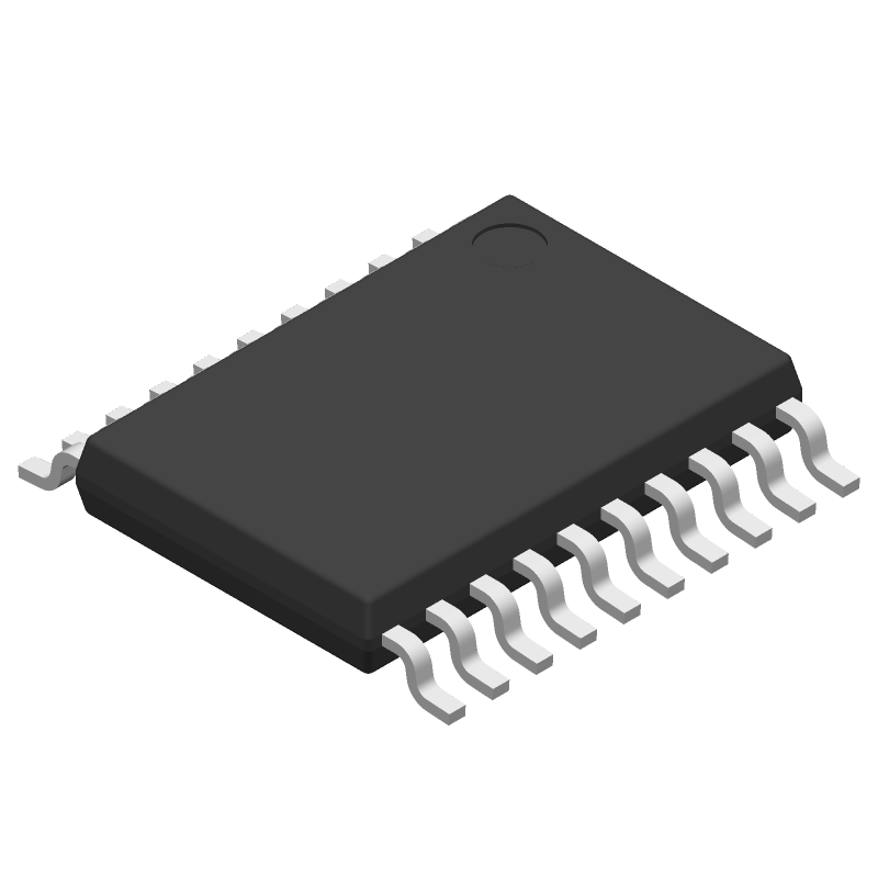
Automotive 12-bit 200-KSPS 11-channel low-power serial ADC with power down 20-TSSOP -40 to 85
Tip: Data for a part may vary between manufacturers. You can filter for manufacturers on the top of the page next to the part image and part number.
TLV2553IPWRQ1 by Texas Instruments is an Analog to Digital Converter.
Analog to Digital Converters are under the broader part category of Converters.
A converter is an electrical circuit that transforms electric energy into a different form that will support a elecrical load needed by a device. Read more about Converters on our Converters part category page.
| Part # | Manufacturer | Description | Datasheet |
|---|---|---|---|
| TLV2553IPWRQ1 | Texas Instruments | Automotive 12-Bit 200-KSPS 11-Channel Low-Power Serial ADC 20-TSSOP -40 to 85 |
| Part # | Distributor | Description | Stock | Price | Buy | |
|---|---|---|---|---|---|---|
|
DISTI #
296-42359-1-ND
|
DigiKey | IC ADC 12BIT SAR 20TSSOP Min Qty: 1 Lead time: 18 Weeks Container: Cut Tape (CT), Tape & Reel (TR), Digi-Reel® |
1285 In Stock |
|
$7.3428 / $12.1900 | Buy Now |
|
DISTI #
595-TLV2553IPWRQ1
|
Mouser Electronics | Analog to Digital Converters - ADC Automotive 12-bit 20 0-KSPS 11-channel lo RoHS: Compliant | 0 |
|
$7.3400 | Order Now |
|
|
Cytech Systems Limited | IC ADC 12BIT SAR 20TSSOP | 2000 |
|
RFQ | |
|
|
Vyrian | Converters | 914 |
|
RFQ |
By downloading CAD models, you agree to our Terms & Conditions and Privacy Policy
|
|
TLV2553IPWRQ1
Texas Instruments
Buy Now
Datasheet
|
Compare Parts:
TLV2553IPWRQ1
Texas Instruments
Automotive 12-bit 200-KSPS 11-channel low-power serial ADC with power down 20-TSSOP -40 to 85
|
| Pbfree Code | Yes | |
| Rohs Code | Yes | |
| Part Life Cycle Code | Active | |
| Ihs Manufacturer | TEXAS INSTRUMENTS INC | |
| Part Package Code | TSSOP | |
| Package Description | TSSOP-20 | |
| Pin Count | 20 | |
| Reach Compliance Code | compliant | |
| ECCN Code | EAR99 | |
| Samacsys Manufacturer | Texas Instruments | |
| Analog Input Voltage-Max | 5.5 V | |
| Analog Input Voltage-Min | ||
| Conversion Time-Max | 5.54 µs | |
| Converter Type | ADC, SUCCESSIVE APPROXIMATION | |
| JESD-30 Code | R-PDSO-G20 | |
| JESD-609 Code | e4 | |
| Length | 6.5 mm | |
| Linearity Error-Max (EL) | 0.0244% | |
| Moisture Sensitivity Level | 3 | |
| Number of Analog In Channels | 11 | |
| Number of Bits | 12 | |
| Number of Functions | 1 | |
| Number of Terminals | 20 | |
| Operating Temperature-Max | 85 °C | |
| Operating Temperature-Min | -40 °C | |
| Output Bit Code | BINARY, 2'S COMPLEMENT BINARY | |
| Output Format | SERIAL | |
| Package Body Material | PLASTIC/EPOXY | |
| Package Code | TSSOP | |
| Package Shape | RECTANGULAR | |
| Package Style | SMALL OUTLINE, THIN PROFILE, SHRINK PITCH | |
| Peak Reflow Temperature (Cel) | 260 | |
| Sample Rate | 0.2 MHz | |
| Sample and Hold / Track and Hold | SAMPLE | |
| Screening Level | AEC-Q100 | |
| Seated Height-Max | 1.2 mm | |
| Supply Current-Max | 1.2 mA | |
| Supply Voltage-Min | 2.7 V | |
| Supply Voltage-Nom | 5 V | |
| Surface Mount | YES | |
| Temperature Grade | INDUSTRIAL | |
| Terminal Finish | Nickel/Palladium/Gold (Ni/Pd/Au) | |
| Terminal Form | GULL WING | |
| Terminal Pitch | 0.65 mm | |
| Terminal Position | DUAL | |
| Time@Peak Reflow Temperature-Max (s) | 30 | |
| Width | 4.4 mm |
A good PCB layout for TLV2553IPWRQ1 involves keeping the analog and digital grounds separate, using a solid ground plane, and placing the device close to the power supply. Additionally, it's recommended to use a 4-layer PCB with a dedicated power plane and a dedicated ground plane.
To ensure the stability of the output voltage, it's essential to use a suitable output capacitor with a low equivalent series resistance (ESR). A ceramic capacitor with a value between 10uF to 22uF is recommended. Additionally, the output capacitor should be placed close to the device to minimize the loop area and reduce noise.
The maximum input voltage that TLV2553IPWRQ1 can handle is 18V. Exceeding this voltage may damage the device. It's recommended to use a voltage regulator or a voltage limiter to ensure that the input voltage remains within the specified range.
To reduce the noise and ripple in the output voltage, it's recommended to use a low-noise input voltage, add a noise filter capacitor (e.g., 10nF) between the input and ground, and use a high-quality output capacitor with low ESR. Additionally, minimizing the loop area and using a shielded cable can also help reduce noise and ripple.
The thermal derating of TLV2553IPWRQ1 is 12.5mW/°C above 25°C. This means that the device's power dissipation should be reduced by 12.5mW for every degree Celsius above 25°C to prevent overheating and ensure reliable operation.