-
Part Symbol
-
Footprint
-
3D Model
Available Download Formats
By downloading CAD models, you agree to our Terms & Conditions and Privacy Policy
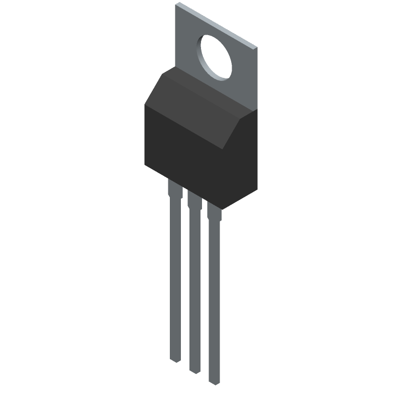
N-channel 650 V, 1.2 Ohm typ., 4 A MDmesh M2 Power MOSFET in TO-220FP package
Tip: Data for a part may vary between manufacturers. You can filter for manufacturers on the top of the page next to the part image and part number.
STF6N65M2 by STMicroelectronics is a Power Field-Effect Transistor.
Power Field-Effect Transistors are under the broader part category of Transistors.
A transistor is a small semiconductor device used to amplify, control, or create electrical signals. When selecting a transistor, factors such as voltage, current rating, gain, and power dissipation must be considered, with common types. Read more about Transistors on our Transistors part category page.
| Part # | Distributor | Description | Stock | Price | Buy | |
|---|---|---|---|---|---|---|
|
DISTI #
40Y2601
|
Newark | Power Mosfet, N Channel, 4 A, 650 V, 1.2 Ohm, 10 V, 3 V Rohs Compliant: Yes |Stmicroelectronics STF6N65M2 RoHS: Compliant Min Qty: 1 Package Multiple: 1 Date Code: 1 Container: Bulk | 1707 |
|
$0.9970 / $1.4500 | Buy Now |
|
DISTI #
497-15035-5-ND
|
DigiKey | MOSFET N-CH 650V 4A TO220FP Min Qty: 1 Lead time: 14 Weeks Container: Tube |
285 In Stock |
|
$0.5813 / $0.9800 | Buy Now |
|
DISTI #
STF6N65M2
|
Avnet Americas | Trans MOSFET N-CH 650V 4A 3-Pin TO-220 FP Tube - Rail/Tube (Alt: STF6N65M2) RoHS: Compliant Min Qty: 2000 Package Multiple: 1000 Lead time: 111 Weeks, 0 Days Container: Tube | 0 |
|
RFQ | |
|
DISTI #
V79:2366_22599300
|
Arrow Electronics | Trans MOSFET N-CH 650V 4A 3-Pin(3+Tab) TO-220FP Tube Min Qty: 1 Package Multiple: 1 Date Code: 1623 | Americas - 400 |
|
$0.5926 | Buy Now |
|
|
STMicroelectronics | N-channel 650 V, 1.2 Ohm typ., 4 A MDmesh M2 Power MOSFET in TO-220FP package COO: China RoHS: Compliant Min Qty: 1 | 1596 |
|
$0.5900 / $0.8600 | Buy Now |
|
DISTI #
30318528
|
Verical | Trans MOSFET N-CH 650V 4A 3-Pin(3+Tab) TO-220FP Tube Min Qty: 10 Package Multiple: 1 Date Code: 1623 | Americas - 400 |
|
$0.5926 | Buy Now |
|
|
Bristol Electronics | 100 |
|
RFQ | ||
|
|
Quest Components | 80 |
|
$1.7160 / $3.1200 | Buy Now | |
|
DISTI #
STF6N65M2
|
TME | Transistor: N-MOSFET, unipolar Min Qty: 1 | 0 |
|
$0.7100 / $1.1900 | RFQ |
|
DISTI #
STF6N65M2
|
Avnet Silica | Trans MOSFET NCH 650V 4A 3Pin TO220 FP Tube (Alt: STF6N65M2) RoHS: Compliant Min Qty: 2000 Package Multiple: 50 Lead time: 15 Weeks, 0 Days | Silica - 0 |
|
Buy Now |
By downloading CAD models, you agree to our Terms & Conditions and Privacy Policy
|
|
STF6N65M2
STMicroelectronics
Buy Now
Datasheet
|
Compare Parts:
STF6N65M2
STMicroelectronics
N-channel 650 V, 1.2 Ohm typ., 4 A MDmesh M2 Power MOSFET in TO-220FP package
|
| Rohs Code | Yes | |
| Part Life Cycle Code | End Of Life | |
| Ihs Manufacturer | STMICROELECTRONICS | |
| Package Description | TO-220FP, 3 PIN | |
| Reach Compliance Code | not_compliant | |
| ECCN Code | EAR99 | |
| Factory Lead Time | 111 Weeks | |
| Samacsys Manufacturer | STMicroelectronics | |
| Avalanche Energy Rating (Eas) | 100 mJ | |
| Case Connection | ISOLATED | |
| Configuration | SINGLE WITH BUILT-IN DIODE | |
| DS Breakdown Voltage-Min | 650 V | |
| Drain Current-Max (ID) | 4 A | |
| Drain-source On Resistance-Max | 1.35 Ω | |
| FET Technology | METAL-OXIDE SEMICONDUCTOR | |
| Feedback Cap-Max (Crss) | 0.65 pF | |
| JEDEC-95 Code | TO-220AB | |
| JESD-30 Code | R-PSFM-T3 | |
| Number of Elements | 1 | |
| Number of Terminals | 3 | |
| Operating Mode | ENHANCEMENT MODE | |
| Operating Temperature-Max | 150 °C | |
| Operating Temperature-Min | -55 °C | |
| Package Body Material | PLASTIC/EPOXY | |
| Package Shape | RECTANGULAR | |
| Package Style | FLANGE MOUNT | |
| Peak Reflow Temperature (Cel) | NOT SPECIFIED | |
| Polarity/Channel Type | N-CHANNEL | |
| Power Dissipation-Max (Abs) | 20 W | |
| Pulsed Drain Current-Max (IDM) | 16 A | |
| Surface Mount | NO | |
| Terminal Form | THROUGH-HOLE | |
| Terminal Position | SINGLE | |
| Time@Peak Reflow Temperature-Max (s) | NOT SPECIFIED | |
| Transistor Application | SWITCHING | |
| Transistor Element Material | SILICON |
The maximum safe operating area (SOA) for the STF6N65M2 is not explicitly stated in the datasheet, but it can be estimated based on the device's thermal and electrical characteristics. A safe operating area can be defined as the region where the device can operate without exceeding its maximum ratings. For the STF6N65M2, this region is typically bounded by the maximum drain-source voltage (Vds), maximum drain current (Id), and maximum junction temperature (Tj). Engineers can use simulation tools or consult with STMicroelectronics' application notes to determine the SOA for their specific application.
To ensure the STF6N65M2 is properly biased for optimal performance, engineers should follow the recommended biasing conditions outlined in the datasheet. This includes setting the gate-source voltage (Vgs) within the recommended range (typically 2-5V) and ensuring the drain-source voltage (Vds) is within the maximum rating (650V). Additionally, engineers should consider the device's threshold voltage (Vth) and ensure the gate drive circuitry can provide sufficient current to charge and discharge the gate capacitance quickly. STMicroelectronics' application notes and evaluation boards can provide further guidance on proper biasing and layout techniques.
Thermal management is critical for the STF6N65M2, as excessive junction temperature (Tj) can lead to reduced performance, reliability, and lifespan. Engineers should consider the device's thermal resistance (Rthja), maximum junction temperature (Tj), and power dissipation (Pd) when designing their application. This includes selecting a suitable heat sink, ensuring good thermal interface material (TIM) between the device and heat sink, and optimizing the PCB layout for thermal dissipation. STMicroelectronics provides thermal management guidelines and recommendations in their application notes and datasheets.
Electrostatic discharge (ESD) can damage the STF6N65M2, so engineers should take precautions to prevent ESD events during handling, assembly, and operation. This includes using ESD-safe materials, equipment, and workstations, as well as following proper handling and storage procedures. Additionally, engineers can implement ESD protection circuits, such as TVS diodes or ESD protection arrays, to protect the device from ESD events. STMicroelectronics provides ESD handling and protection guidelines in their application notes and datasheets.
Proper PCB layout and routing are crucial for the STF6N65M2 to ensure optimal performance, reduce electromagnetic interference (EMI), and prevent thermal issues. Engineers should follow STMicroelectronics' recommended PCB layout and routing guidelines, which include keeping the drain and source pins separate, using a solid ground plane, and minimizing trace lengths and inductance. Additionally, engineers should consider the device's pinout, thermal vias, and heat sink attachment when designing their PCB layout.