-
Part Symbol
-
Footprint
-
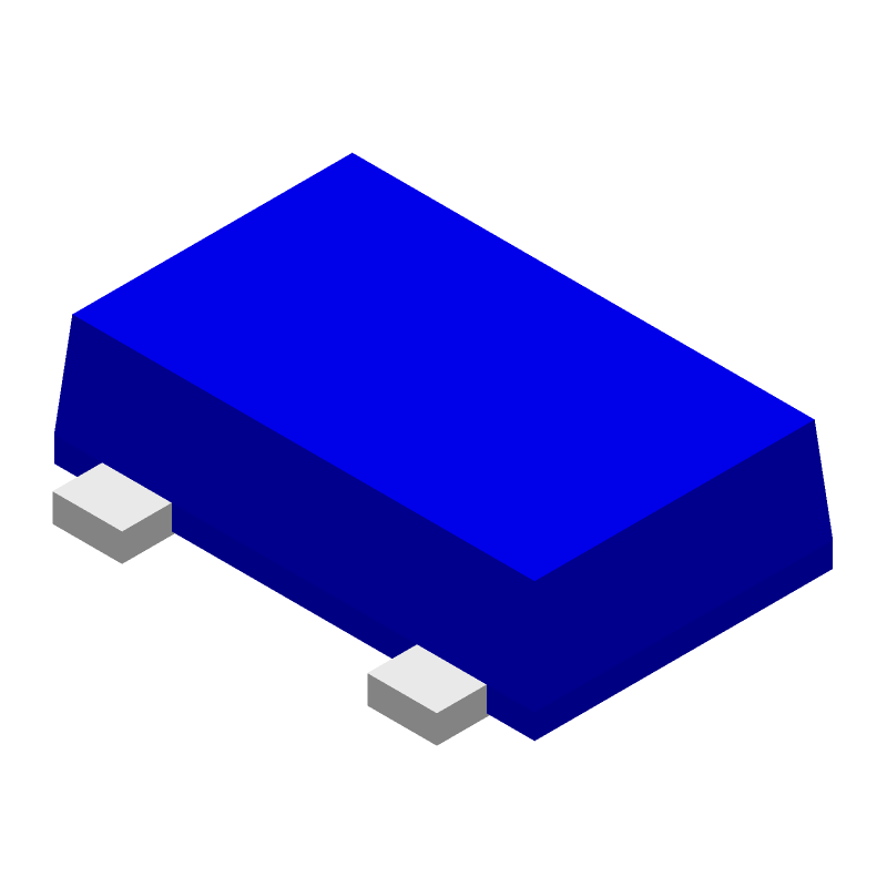
3D Model
Available Download Formats
By downloading CAD models, you agree to our Terms & Conditions and Privacy Policy
Transistors (Bipolar/MOSFETs/IGBTs) - MOSFETs - Junction FETs (Single/Dual) - Small-Signal MOSFETs(Single)
Tip: Data for a part may vary between manufacturers. You can filter for manufacturers on the top of the page next to the part image and part number.
SSM3K339R by Toshiba America Electronic Components is a Power Field-Effect Transistor.
Power Field-Effect Transistors are under the broader part category of Transistors.
A transistor is a small semiconductor device used to amplify, control, or create electrical signals. When selecting a transistor, factors such as voltage, current rating, gain, and power dissipation must be considered, with common types. Read more about Transistors on our Transistors part category page.
| Part # | Distributor | Description | Stock | Price | Buy | |
|---|---|---|---|---|---|---|
|
DISTI #
SSM3K339R
|
TME | Transistor: N-MOSFET, unipolar, 40V, 2A, 1W, SOT23F Min Qty: 5 | 5100 |
|
$0.0680 / $0.1440 | Buy Now |
|
|
Win Source Electronics | MOSFETs Silicon N-Channel MOS | 45814 |
|
$0.1460 / $0.2189 | Buy Now |
By downloading CAD models, you agree to our Terms & Conditions and Privacy Policy
|
|
SSM3K339R
Toshiba America Electronic Components
Buy Now
Datasheet
|
Compare Parts:
SSM3K339R
Toshiba America Electronic Components
Transistors (Bipolar/MOSFETs/IGBTs) - MOSFETs - Junction FETs (Single/Dual) - Small-Signal MOSFETs(Single)
|
| Rohs Code | Yes | |
| Part Life Cycle Code | Active | |
| Ihs Manufacturer | TOSHIBA CORP | |
| Package Description | SOT-23F, 3 PIN | |
| Reach Compliance Code | compliant | |
| ECCN Code | EAR99 | |
| Factory Lead Time | 16 Weeks | |
| Samacsys Manufacturer | Toshiba | |
| Configuration | SINGLE WITH BUILT-IN DIODE | |
| DS Breakdown Voltage-Min | 40 V | |
| Drain Current-Max (ID) | 2 A | |
| Drain-source On Resistance-Max | 0.208 Ω | |
| FET Technology | METAL-OXIDE SEMICONDUCTOR | |
| Feedback Cap-Max (Crss) | 7.5 pF | |
| JESD-30 Code | R-PDSO-F3 | |
| Number of Elements | 1 | |
| Number of Terminals | 3 | |
| Operating Mode | ENHANCEMENT MODE | |
| Operating Temperature-Max | 150 °C | |
| Package Body Material | PLASTIC/EPOXY | |
| Package Shape | RECTANGULAR | |
| Package Style | SMALL OUTLINE | |
| Peak Reflow Temperature (Cel) | NOT SPECIFIED | |
| Polarity/Channel Type | N-CHANNEL | |
| Power Dissipation-Max (Abs) | 1 W | |
| Pulsed Drain Current-Max (IDM) | 4 A | |
| Surface Mount | YES | |
| Terminal Form | FLAT | |
| Terminal Position | DUAL | |
| Time@Peak Reflow Temperature-Max (s) | NOT SPECIFIED | |
| Transistor Application | SWITCHING | |
| Transistor Element Material | SILICON |
A 2-layer or 4-layer PCB with a thermal relief pattern and a solid ground plane is recommended. Ensure that the thermal pad is connected to a large copper area to dissipate heat efficiently.
Ensure that the input voltage is within the recommended range (1.8V to 5.5V) and that the enable pin is properly biased (high or low) according to the application requirements.
The maximum allowable power dissipation is 1.5W. Ensure that the device is properly heat-sinked and that the ambient temperature is within the recommended range (-40°C to 125°C).
Yes, the SSM3K339R is AEC-Q100 qualified and suitable for high-reliability and automotive applications. However, ensure that the device is properly qualified and validated for the specific application requirements.
The POR and BOR features are enabled by default. Ensure that the power supply is stable and within the recommended range to prevent unwanted resets. You can also disable these features by tying the POR/BOR pins to VCC or GND, respectively.