-
Part Symbol
-
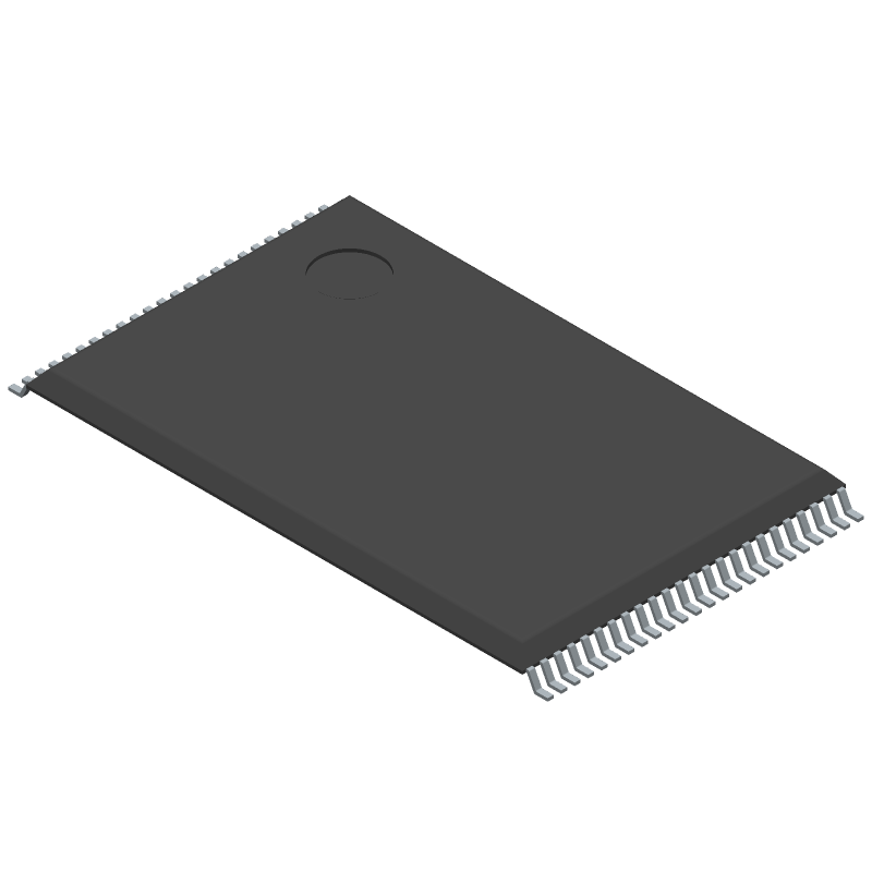
Footprint
-
3D Model
Available Download Formats
By downloading CAD models, you agree to our Terms & Conditions and Privacy Policy
Flash, 8MX8, 70ns, PDSO48,
Tip: Data for a part may vary between manufacturers. You can filter for manufacturers on the top of the page next to the part image and part number.
S29GL064S70TFI070 by Infineon Technologies AG is a Flash Memory.
Flash Memories are under the broader part category of Memory Components.
Memory components are essential in electronics for computer processing. They can be volatile or non-volatile, depending on the desired function. Read more about Memory Components on our Memory part category page.
| Part # | Distributor | Description | Stock | Price | Buy | |
|---|---|---|---|---|---|---|
|
DISTI #
62AK5990
|
Newark | Flash Memory, 64Mbit, 85Deg C, Tsop-48, Flash Memory Type:Parallel Nor, Memory Configuration:4M X 16Bit, Interfaces:Parallel, Ic Case/Package:Tsop, No. Of Pins:48Pins, Clock Frequency Max:-, Access Time:70Ns, Supply Voltage Nom:- Rohs Compliant: Yes |Infineon S29GL064S70TFI070 RoHS: Compliant Min Qty: 1 Package Multiple: 1 Date Code: 0 Container: Bulk | 960 |
|
$3.1100 / $3.8200 | Buy Now |
|
DISTI #
S29GL064S70TFI070-ND
|
DigiKey | IC FLASH 64MBIT PARALLEL 56TSOP Min Qty: 1 Lead time: 10 Weeks Container: Tray |
782 In Stock |
|
$3.3551 / $4.2400 | Buy Now |
|
DISTI #
727-S29GL064S70TFI07
|
Mouser Electronics | NOR Flash PNOR RoHS: Compliant | 1190 |
|
$3.0800 / $4.2400 | Buy Now |
|
DISTI #
84875701
|
Verical | 64M bit 3V-ONLY, PAGE-MODE FLASH MEMORY RoHS: Compliant Min Qty: 2 Package Multiple: 1 Date Code: 2429 | Americas - 5369 |
|
$2.9577 / $3.7521 | Buy Now |
|
DISTI #
82120435
|
Verical | 64M bit 3V-ONLY, PAGE-MODE FLASH MEMORY RoHS: Compliant Min Qty: 10 Package Multiple: 1 Date Code: 2417 | Americas - 860 |
|
$3.1900 / $4.2000 | Buy Now |
|
DISTI #
87801880
|
Verical | 64M bit 3V-ONLY, PAGE-MODE FLASH MEMORY RoHS: Compliant Min Qty: 111 Package Multiple: 1 Date Code: 2201 | Americas - 129 |
|
$2.8500 / $3.3875 | Buy Now |
|
|
Rochester Electronics | (8 Mbyte), 3.0V, Flash Memory RoHS: Compliant Status: Active Min Qty: 1 | 472 |
|
$2.2800 / $2.8500 | Buy Now |
|
DISTI #
S29GL064S70TFI070
|
Chip One Stop | Semiconductors RoHS: Compliant pbFree: Yes Min Qty: 1 Lead time: 0 Weeks, 1 Days Container: Tray | 860 |
|
$3.1300 / $4.2000 | Buy Now |
|
DISTI #
SP005664963
|
EBV Elektronik | (Alt: SP005664963) RoHS: Compliant Min Qty: 960 Package Multiple: 960 Lead time: 11 Weeks, 0 Days | EBV - 0 |
|
Buy Now |
By downloading CAD models, you agree to our Terms & Conditions and Privacy Policy
|
|
S29GL064S70TFI070
Infineon Technologies AG
Buy Now
Datasheet
|
Compare Parts:
S29GL064S70TFI070
Infineon Technologies AG
Flash, 8MX8, 70ns, PDSO48,
|
| Rohs Code | Yes | |
| Part Life Cycle Code | Active | |
| Ihs Manufacturer | INFINEON TECHNOLOGIES AG | |
| Package Description | TSOP-48 | |
| Reach Compliance Code | compliant | |
| Factory Lead Time | 4 Weeks | |
| Samacsys Manufacturer | Infineon | |
| Access Time-Max | 70 ns | |
| Alternate Memory Width | 8 | |
| Boot Block | BOTTOM/TOP | |
| Command User Interface | YES | |
| Common Flash Interface | YES | |
| Data Polling | YES | |
| Data Retention Time-Min | 20 | |
| Endurance | 1000000 Write/Erase Cycles | |
| JESD-30 Code | R-PDSO-G48 | |
| JESD-609 Code | e3 | |
| Length | 18.4 mm | |
| Memory Density | 67108864 bit | |
| Memory IC Type | FLASH | |
| Memory Width | 16 | |
| Moisture Sensitivity Level | 3 | |
| Number of Functions | 1 | |
| Number of Sectors/Size | 8,127 | |
| Number of Terminals | 48 | |
| Number of Words | 4194304 words | |
| Number of Words Code | 4000000 | |
| Operating Mode | ASYNCHRONOUS | |
| Operating Temperature-Max | 85 °C | |
| Operating Temperature-Min | -40 °C | |
| Organization | 4MX16 | |
| Output Characteristics | 3-STATE | |
| Package Body Material | PLASTIC/EPOXY | |
| Package Code | TSSOP | |
| Package Equivalence Code | TSSOP48,.8,20 | |
| Package Shape | RECTANGULAR | |
| Package Style | SMALL OUTLINE, THIN PROFILE, SHRINK PITCH | |
| Parallel/Serial | PARALLEL | |
| Programming Voltage | 3 V | |
| Ready/Busy | YES | |
| Reverse Pinout | NO | |
| Seated Height-Max | 1.2 mm | |
| Sector Size | 8K,64K | |
| Standby Current-Max | 0.0001 A | |
| Supply Current-Max | 0.06 mA | |
| Supply Voltage-Max (Vsup) | 3.6 V | |
| Supply Voltage-Min (Vsup) | 2.7 V | |
| Supply Voltage-Nom (Vsup) | 3 V | |
| Surface Mount | YES | |
| Technology | CMOS | |
| Temperature Grade | INDUSTRIAL | |
| Terminal Finish | Matte Tin (Sn) | |
| Terminal Form | GULL WING | |
| Terminal Pitch | 0.5 mm | |
| Terminal Position | DUAL | |
| Toggle Bit | YES | |
| Type | NOR TYPE | |
| Width | 12 mm | |
| Write Cycle Time-Max (tWC) | 0.00006 ms | |
| Write Protection | HARDWARE/SOFTWARE |
This table gives cross-reference parts and alternative options found for S29GL064S70TFI070. The Form Fit Function (FFF) tab will give you the options that are more likely to serve as direct pin-to-pin alternates or drop-in parts. The Functional Equivalents tab will give you options that are likely to match the same function of S29GL064S70TFI070, but it may not fit your design. Always verify details of parts you are evaluating, as these parts are offered as suggestions for what you are looking for and are not guaranteed.
| Part Number | Manufacturer | Composite Price | Description | Compare |
|---|---|---|---|---|
| S29GL064S70TFI073 | Cypress Semiconductor | Check for Price | Flash, 8MX8, 70ns, PDSO48, TSOP-48 | S29GL064S70TFI070 vs S29GL064S70TFI073 |
| S29GL064S70TFA073 | Cypress Semiconductor | Check for Price | Flash, 4MX16, 70ns, PDSO48, TSOP-48 | S29GL064S70TFI070 vs S29GL064S70TFA073 |
| S29GL064S70TFA073 | Infineon Technologies AG | Check for Price | Flash, 4MX16, 70ns, PDSO48, TSOP-48 | S29GL064S70TFI070 vs S29GL064S70TFA073 |
The maximum operating temperature range for the S29GL064S70TFI070 is -40°C to +85°C.
The HOLD# signal should be asserted low to pause the current operation and de-asserted high to resume the operation. During this time, the device will tri-state its outputs and ignore any input signals.
The WP# pin is used to prevent accidental writes to the device. When WP# is asserted low, the device will ignore any write commands and protect the data from being modified.
To perform a sector erase operation, send the erase command (0x60h) followed by the sector address. The device will then erase the entire sector.
The recommended power-up sequence is to apply VCC first, followed by VPP, and then the clock signal. This ensures proper device initialization and prevents latch-up conditions.