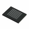
Part Details for PC28F256J3F95A by Micron Technology Inc
Results Overview of PC28F256J3F95A by Micron Technology Inc
- Distributor Offerings: (1 listing)
- Number of FFF Equivalents: (1 replacement)
- CAD Models: (Request Part)
- Number of Functional Equivalents: (10 options)
- Part Data Attributes: (Available)
- Reference Designs: (Not Available)
Tip: Data for a part may vary between manufacturers. You can filter for manufacturers on the top of the page next to the part image and part number.
PC28F256J3F95A Information
PC28F256J3F95A by Micron Technology Inc is a Flash Memory.
Flash Memories are under the broader part category of Memory Components.
Memory components are essential in electronics for computer processing. They can be volatile or non-volatile, depending on the desired function. Read more about Memory Components on our Memory part category page.
Price & Stock for PC28F256J3F95A
| Part # | Distributor | Description | Stock | Price | Buy | |
|---|---|---|---|---|---|---|
|
|
Win Source Electronics | IC FLASH 256MBIT 95NS 64EASYBGA | 2000 |
|
$108.8045 / $129.7284 | Buy Now |
Part Details for PC28F256J3F95A
PC28F256J3F95A CAD Models
PC28F256J3F95A Part Data Attributes
|
|
PC28F256J3F95A
Micron Technology Inc
Buy Now
Datasheet
|
Compare Parts:
PC28F256J3F95A
Micron Technology Inc
Flash, 16MX16, 95ns, PBGA64, LEAD FREE, BGA-64
|
| Pbfree Code | Yes | |
| Rohs Code | Yes | |
| Part Life Cycle Code | Obsolete | |
| Ihs Manufacturer | MICRON TECHNOLOGY INC | |
| Part Package Code | BGA | |
| Package Description | LEAD FREE, BGA-64 | |
| Pin Count | 64 | |
| Reach Compliance Code | compliant | |
| ECCN Code | EAR99 | |
| HTS Code | 8542.32.00.51 | |
| Samacsys Manufacturer | Micron | |
| Access Time-Max | 95 ns | |
| Alternate Memory Width | 8 | |
| JESD-30 Code | R-PBGA-B64 | |
| JESD-609 Code | e1 | |
| Length | 13 mm | |
| Memory Density | 268435456 bit | |
| Memory IC Type | FLASH | |
| Memory Width | 16 | |
| Number of Functions | 1 | |
| Number of Terminals | 64 | |
| Number of Words | 16777216 words | |
| Number of Words Code | 16000000 | |
| Operating Mode | ASYNCHRONOUS | |
| Operating Temperature-Max | 85 °C | |
| Operating Temperature-Min | -40 °C | |
| Organization | 16MX16 | |
| Package Body Material | PLASTIC/EPOXY | |
| Package Code | TBGA | |
| Package Shape | RECTANGULAR | |
| Package Style | GRID ARRAY | |
| Parallel/Serial | PARALLEL | |
| Peak Reflow Temperature (Cel) | 260 | |
| Programming Voltage | 2.7 V | |
| Qualification Status | Not Qualified | |
| Seated Height-Max | 1.2 mm | |
| Supply Voltage-Max (Vsup) | 3.6 V | |
| Supply Voltage-Min (Vsup) | 2.7 V | |
| Supply Voltage-Nom (Vsup) | 3 V | |
| Surface Mount | YES | |
| Technology | CMOS | |
| Temperature Grade | INDUSTRIAL | |
| Terminal Finish | Tin/Silver/Copper (Sn/Ag/Cu) | |
| Terminal Form | BALL | |
| Terminal Pitch | 1 mm | |
| Terminal Position | BOTTOM | |
| Time@Peak Reflow Temperature-Max (s) | 30 | |
| Type | NOR TYPE | |
| Width | 10 mm |
Alternate Parts for PC28F256J3F95A
This table gives cross-reference parts and alternative options found for PC28F256J3F95A. The Form Fit Function (FFF) tab will give you the options that are more likely to serve as direct pin-to-pin alternates or drop-in parts. The Functional Equivalents tab will give you options that are likely to match the same function of PC28F256J3F95A, but it may not fit your design. Always verify details of parts you are evaluating, as these parts are offered as suggestions for what you are looking for and are not guaranteed.
| Part Number | Manufacturer | Composite Price | Description | Compare |
|---|---|---|---|---|
| PC28F256J3F95 | Micron Technology Inc | Check for Price | Flash, 16MX16, 95ns, PBGA64, LEAD FREE, BGA-64 | PC28F256J3F95A vs PC28F256J3F95 |
PC28F256J3F95A Frequently Asked Questions (FAQ)
-
The PC28F256J3F95A has an operating temperature range of -40°C to 85°C.
-
The PC28F256J3F95A is rated for a minimum of 100,000 erase and reprogram cycles.
-
The typical access time for the PC28F256J3F95A is 95ns.
-
The PC28F256J3F95A is a 3.3V device, but it is also 5V tolerant, making it compatible with both 3.3V and 5V systems.
-
The HOLD# signal should be used to pause the flash memory during a read or write operation, while the OE# signal should be used to enable or disable the output drivers.
