-
3D Model
Available Download Formats
By downloading CAD models, you agree to our Terms & Conditions and Privacy Policy

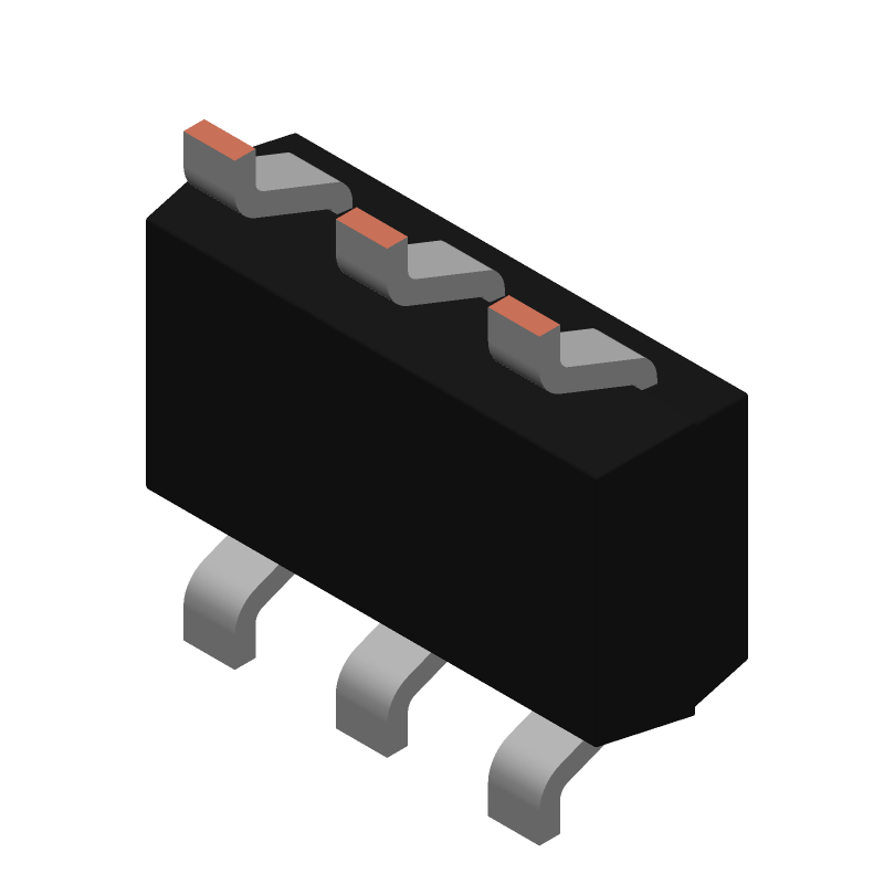
PBSS4140DPN - 40 V low VCEsat NPN/PNP transistor@en-us TSOP 6-Pin
Tip: Data for a part may vary between manufacturers. You can filter for manufacturers on the top of the page next to the part image and part number.
PBSS4140DPNF by Nexperia is a Small Signal Bipolar Transistor.
Small Signal Bipolar Transistors are under the broader part category of Transistors.
A transistor is a small semiconductor device used to amplify, control, or create electrical signals. When selecting a transistor, factors such as voltage, current rating, gain, and power dissipation must be considered, with common types. Read more about Transistors on our Transistors part category page.
| Part # | Distributor | Description | Stock | Price | Buy | |
|---|---|---|---|---|---|---|
|
DISTI #
74AH1019
|
Newark | Bipolar Array, Npn/Pnp, 40V, 1A, Sc74 Rohs Compliant: Yes |Nexperia PBSS4140DPNF RoHS: Compliant Min Qty: 5 Package Multiple: 1 Date Code: 1 Container: Cut Tape | 15868 |
|
$0.1560 / $0.4320 | Buy Now |
|
DISTI #
1727-2759-1-ND
|
DigiKey | TRANS NPN/PNP 40V 1A 6-TSOP Min Qty: 1 Lead time: 8 Weeks Container: Digi-Reel®, Cut Tape (CT), Tape & Reel (TR) |
103083 In Stock |
|
$0.0846 / $0.5400 | Buy Now |
|
DISTI #
PBSS4140DPNF
|
Avnet Americas | PBSS4140DPN/SC-74/REEL 13" Q1/" - Tape and Reel (Alt: PBSS4140DPNF) RoHS: Compliant Min Qty: 10000 Package Multiple: 10000 Lead time: 8 Weeks, 0 Days Container: Reel | 0 |
|
$0.0772 / $0.0907 | Buy Now |
|
DISTI #
771-PBSS4140DPNF
|
Mouser Electronics | Bipolar Transistors - BJT 40 V, 1 A NPN low VCEsat transistor RoHS: Compliant | 13819 |
|
$0.0840 / $0.3800 | Buy Now |
|
DISTI #
PBSS4140DPNF
|
TTI | Bipolar Transistors - BJT 40 V, 1 A NPN low VCEsat transistor RoHS: Compliant pbFree: Pb-Free Min Qty: 10000 Package Multiple: 10000 Container: Reel | Americas - 0 |
|
$0.1960 | Buy Now |
|
DISTI #
PBSS4140DPNF
|
TTI | Bipolar Transistors - BJT 40 V, 1 A NPN low VCEsat transistor RoHS: Compliant pbFree: Pb-Free Min Qty: 10000 Package Multiple: 10000 Container: Reel | Americas - 0 |
|
$0.1960 | Buy Now |
|
DISTI #
PBSS4140DPNF
|
TME | Transistor: NPN / PNP, bipolar, complementary pair, 40V, 1A, 370mW Min Qty: 1 | 0 |
|
$0.1260 / $0.3450 | RFQ |
|
DISTI #
PBSS4140DPNF
|
Avnet Silica | PBSS4140DPNSC74REEL 13 Q1 (Alt: PBSS4140DPNF) RoHS: Compliant Min Qty: 10000 Package Multiple: 10000 Lead time: 10 Weeks, 0 Days | Silica - 0 |
|
Buy Now | |
|
DISTI #
PBSS4140DPNF
|
EBV Elektronik | PBSS4140DPNSC74REEL 13 Q1 (Alt: PBSS4140DPNF) RoHS: Compliant Min Qty: 10000 Package Multiple: 10000 Lead time: 10 Weeks, 0 Days | EBV - 0 |
|
Buy Now |
By downloading CAD models, you agree to our Terms & Conditions and Privacy Policy
|
|
PBSS4140DPNF
Nexperia
Buy Now
Datasheet
|
Compare Parts:
PBSS4140DPNF
Nexperia
PBSS4140DPN - 40 V low VCEsat NPN/PNP transistor@en-us TSOP 6-Pin
|
| Rohs Code | Yes | |
| Part Life Cycle Code | Active | |
| Ihs Manufacturer | NEXPERIA | |
| Part Package Code | TSOP | |
| Package Description | PLASTIC, SC-74, 6 PIN | |
| Pin Count | 6 | |
| Manufacturer Package Code | SOT457 | |
| Reach Compliance Code | compliant | |
| ECCN Code | EAR99 | |
| Factory Lead Time | 8 Weeks | |
| Samacsys Manufacturer | Nexperia | |
| Collector Current-Max (IC) | 1 A | |
| Collector-Emitter Voltage-Max | 40 V | |
| Configuration | SEPARATE, 2 ELEMENTS | |
| DC Current Gain-Min (hFE) | 200 | |
| JESD-30 Code | R-PDSO-G6 | |
| JESD-609 Code | e3 | |
| Moisture Sensitivity Level | 1 | |
| Number of Elements | 2 | |
| Number of Terminals | 6 | |
| Package Body Material | PLASTIC/EPOXY | |
| Package Shape | RECTANGULAR | |
| Package Style | SMALL OUTLINE | |
| Peak Reflow Temperature (Cel) | 260 | |
| Polarity/Channel Type | NPN AND PNP | |
| Surface Mount | YES | |
| Terminal Finish | TIN | |
| Terminal Form | GULL WING | |
| Terminal Position | DUAL | |
| Time@Peak Reflow Temperature-Max (s) | 30 | |
| Transistor Application | SWITCHING | |
| Transistor Element Material | SILICON | |
| Transition Frequency-Nom (fT) | 150 MHz |
The recommended PCB footprint for PBSS4140DPNF is a standard SOT23 package with a 1.5 mm x 1.5 mm body size and a 0.5 mm lead pitch. A minimum pad size of 0.6 mm x 0.6 mm is recommended for reliable soldering.
To ensure reliable operation of PBSS4140DPNF in high-temperature environments, it is recommended to derate the maximum power dissipation according to the temperature derating curve provided in the datasheet. Additionally, ensure good thermal design and heat sinking to keep the junction temperature below 150°C.
The maximum allowed voltage on the input pins of PBSS4140DPNF is 6.5V. Exceeding this voltage may cause damage to the device.
Yes, PBSS4140DPNF can be used in switching applications. However, it is essential to ensure that the device is operated within the recommended switching frequency range (up to 100 kHz) and that the output is properly decoupled to prevent oscillations.
To prevent ESD damage, handle PBSS4140DPNF with ESD-protective equipment and follow proper ESD handling procedures. Ensure that the device is stored in an ESD-protective package and that all personnel handling the device are grounded.