-
Part Symbol
-
Footprint
-
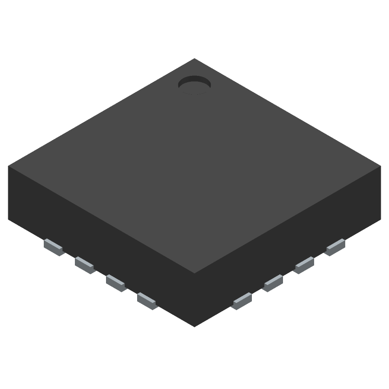
3D Model
Available Download Formats
By downloading CAD models, you agree to our Terms & Conditions and Privacy Policy
2.7GHz, 5V, Low Noise, Rail-to-Rail Input Differential Amplifier/Driver
Tip: Data for a part may vary between manufacturers. You can filter for manufacturers on the top of the page next to the part image and part number.
LTC6405IUD#PBF by Analog Devices Inc is an Operational Amplifier.
Operational Amplifiers are under the broader part category of Amplifier Circuits.
Amplifier circuits use external power to increase the amplitude of an input signal. They can be used to perform linear amplifications or logarithmic functions. Read more about Amplifier Circuits on our Amplifier Circuits part category page.
| Part # | Distributor | Description | Stock | Price | Buy | |
|---|---|---|---|---|---|---|
|
DISTI #
4019160
|
Farnell | DIFF-AMP, 2.7GHZ, -40 TO 85DEG C, QFN-16 RoHS: Compliant Min Qty: 1 Lead time: 11 Weeks, 1 Days Container: Each | 105 |
|
$6.4063 / $12.2302 | Buy Now |
|
DISTI #
V36:1790_06491560
|
Arrow Electronics | SP Amp DIFF AMP Single R-R I/P 5.5V 16-Pin QFN EP Tube RoHS: Compliant Min Qty: 121 Package Multiple: 121 Lead time: 10 Weeks Date Code: 2226 | Americas - 67 |
|
$5.7560 | Buy Now |
|
|
Win Source Electronics | IC ADC DRIVER 16QFN / ADC Driver IC Data Acquisition 16-QFN (3x3) | 2460 |
|
$12.0955 / $18.1432 | Buy Now |
By downloading CAD models, you agree to our Terms & Conditions and Privacy Policy
|
|
LTC6405IUD#PBF
Analog Devices Inc
Buy Now
Datasheet
|
Compare Parts:
LTC6405IUD#PBF
Analog Devices Inc
2.7GHz, 5V, Low Noise, Rail-to-Rail Input Differential Amplifier/Driver
|
| Pbfree Code | No | |
| Rohs Code | Yes | |
| Part Life Cycle Code | Obsolete | |
| Ihs Manufacturer | ANALOG DEVICES INC | |
| Package Description | QFN-16 | |
| Pin Count | 16 | |
| Manufacturer Package Code | 05-08-1691 | |
| Reach Compliance Code | compliant | |
| ECCN Code | EAR99 | |
| HTS Code | 8542.33.00.01 | |
| Samacsys Manufacturer | Analog Devices | |
| Amplifier Type | OPERATIONAL AMPLIFIER | |
| Architecture | VOLTAGE-FEEDBACK | |
| Bandwidth (3dB)-Nom | 800 MHz | |
| Common-mode Reject Ratio-Min | 50 dB | |
| Common-mode Reject Ratio-Nom | 75 dB | |
| Frequency Compensation | YES | |
| Input Offset Current-Max (IIO) | 4 µA | |
| Input Offset Voltage-Max | 7000 µV | |
| JESD-30 Code | S-PQCC-N16 | |
| JESD-609 Code | e3 | |
| Length | 3 mm | |
| Low-Bias | NO | |
| Low-Offset | NO | |
| Micropower | NO | |
| Moisture Sensitivity Level | 1 | |
| Number of Functions | 1 | |
| Number of Terminals | 16 | |
| Operating Temperature-Max | 85 °C | |
| Operating Temperature-Min | -40 °C | |
| Package Body Material | PLASTIC/EPOXY | |
| Package Code | HVQCCN | |
| Package Equivalence Code | LCC16,.12SQ,20 | |
| Package Shape | SQUARE | |
| Package Style | CHIP CARRIER, HEAT SINK/SLUG, VERY THIN PROFILE | |
| Peak Reflow Temperature (Cel) | 260 | |
| Power | NO | |
| Programmable Power | NO | |
| Seated Height-Max | 0.8 mm | |
| Slew Rate-Nom | 690 V/us | |
| Supply Current-Max | 23 mA | |
| Supply Voltage Limit-Max | 5.5 V | |
| Supply Voltage-Nom (Vsup) | 5 V | |
| Surface Mount | YES | |
| Technology | CMOS | |
| Temperature Grade | INDUSTRIAL | |
| Terminal Finish | Matte Tin (Sn) | |
| Terminal Form | NO LEAD | |
| Terminal Pitch | 0.5 mm | |
| Terminal Position | QUAD | |
| Time@Peak Reflow Temperature-Max (s) | 30 | |
| Unity Gain BW-Nom | 2700000 | |
| Wideband | YES | |
| Width | 3 mm |
This table gives cross-reference parts and alternative options found for LTC6405IUD#PBF. The Form Fit Function (FFF) tab will give you the options that are more likely to serve as direct pin-to-pin alternates or drop-in parts. The Functional Equivalents tab will give you options that are likely to match the same function of LTC6405IUD#PBF, but it may not fit your design. Always verify details of parts you are evaluating, as these parts are offered as suggestions for what you are looking for and are not guaranteed.
| Part Number | Manufacturer | Composite Price | Description | Compare |
|---|---|---|---|---|
| LTC6405IUD | Analog Devices Inc | Check for Price | Operational Amplifier, 1 Func, CMOS, PQCC16 | LTC6405IUD#PBF vs LTC6405IUD |
| LTC6405IMS8E#TR | Analog Devices Inc | Check for Price | Operational Amplifier, 1 Func, CMOS, PDSO8 | LTC6405IUD#PBF vs LTC6405IMS8E#TR |
| LTC6405CMS8E#TRPBF | Analog Devices Inc | Check for Price | 2.7GHz, 5V, Low Noise, Rail-to-Rail Input Differential Amplifier/Driver | LTC6405IUD#PBF vs LTC6405CMS8E#TRPBF |
| LTC6405IMS8E | Analog Devices Inc | Check for Price | Operational Amplifier, 1 Func, CMOS, PDSO8 | LTC6405IUD#PBF vs LTC6405IMS8E |
A good PCB layout for the LTC6405 involves keeping the input and output traces short and away from each other, using a solid ground plane, and placing the input and output capacitors close to the device. A 4-layer PCB with a dedicated ground plane is recommended.
To ensure stability, make sure to follow the recommended component values and PCB layout guidelines. Also, ensure that the input and output capacitors are of high quality and have low ESR. Additionally, a small resistor (e.g., 10Ω) in series with the output can help dampen oscillations.
The maximum power dissipation of the LTC6405 is dependent on the package type and thermal environment. For the UD package, the maximum power dissipation is approximately 1.4W at 25°C ambient temperature. However, this can be increased with proper heat sinking and airflow.
While the LTC6405 is primarily a high-speed amplifier, it can be used as a voltage regulator in certain applications. However, it's essential to ensure that the output voltage is within the device's specified range and that the input voltage is sufficient to maintain regulation.
To protect the LTC6405 from overvoltage and ESD, use a voltage clamp or a transient voltage suppressor (TVS) diode at the input. Additionally, follow proper ESD handling procedures during assembly and storage.