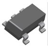
Part Details for LTC2050HVIS5#TRMPBF by Linear Technology
Results Overview of LTC2050HVIS5#TRMPBF by Linear Technology
- Distributor Offerings: (4 listings)
- Number of FFF Equivalents: (0 replacements)
- CAD Models: (Request Part)
- Number of Functional Equivalents: (0 options)
- Part Data Attributes: (Available)
- Reference Designs: (Not Available)
Tip: Data for a part may vary between manufacturers. You can filter for manufacturers on the top of the page next to the part image and part number.
LTC2050HVIS5#TRMPBF Information
LTC2050HVIS5#TRMPBF by Linear Technology is an Operational Amplifier.
Operational Amplifiers are under the broader part category of Amplifier Circuits.
Amplifier circuits use external power to increase the amplitude of an input signal. They can be used to perform linear amplifications or logarithmic functions. Read more about Amplifier Circuits on our Amplifier Circuits part category page.
Price & Stock for LTC2050HVIS5#TRMPBF
| Part # | Distributor | Description | Stock | Price | Buy | |
|---|---|---|---|---|---|---|
|
|
Bristol Electronics | 318 |
|
RFQ | ||
|
|
Quest Components | OP-AMP, 3UV OFFSET-MAX, 3MHZ BAND WIDTH, PDSO5 | 8 |
|
$20.5000 | Buy Now |
|
|
Vyrian | Amplifiers | 2743 |
|
RFQ | |
|
|
Win Source Electronics | IC OPAMP CHOPPER 3MHZ TSOT23-5 | 2260 |
|
$4.1709 / $6.2562 | Buy Now |
Part Details for LTC2050HVIS5#TRMPBF
LTC2050HVIS5#TRMPBF CAD Models
LTC2050HVIS5#TRMPBF Part Data Attributes
|
|
LTC2050HVIS5#TRMPBF
Linear Technology
Buy Now
Datasheet
|
Compare Parts:
LTC2050HVIS5#TRMPBF
Linear Technology
LTC2050 - Zero-Drift Operational Amplifiers in SOT-23; Package: SOT; Pins: 5; Temperature Range: -40°C to 85°C
|
| Rohs Code | Yes | |
| Part Life Cycle Code | Transferred | |
| Ihs Manufacturer | LINEAR TECHNOLOGY CORP | |
| Part Package Code | SOT | |
| Package Description | LEAD FREE, PLASTIC, MO-193, TSOT-23, 5 PIN | |
| Pin Count | 5 | |
| Manufacturer Package Code | S5 | |
| Reach Compliance Code | compliant | |
| ECCN Code | EAR99 | |
| HTS Code | 8542.33.00.01 | |
| Amplifier Type | OPERATIONAL AMPLIFIER | |
| Average Bias Current-Max (IIB) | 0.0003 µA | |
| Common-mode Reject Ratio-Nom | 130 dB | |
| Input Offset Voltage-Max | 3 µV | |
| JESD-30 Code | R-PDSO-G5 | |
| JESD-609 Code | e3 | |
| Length | 2.9 mm | |
| Moisture Sensitivity Level | 1 | |
| Neg Supply Voltage Limit-Max | -6 V | |
| Neg Supply Voltage-Nom (Vsup) | -5 V | |
| Number of Functions | 1 | |
| Number of Terminals | 5 | |
| Operating Temperature-Max | 85 °C | |
| Operating Temperature-Min | -40 °C | |
| Package Body Material | PLASTIC/EPOXY | |
| Package Code | VSSOP | |
| Package Shape | RECTANGULAR | |
| Package Style | SMALL OUTLINE, VERY THIN PROFILE, SHRINK PITCH | |
| Packing Method | TR | |
| Qualification Status | Not Qualified | |
| Seated Height-Max | 1 mm | |
| Slew Rate-Nom | 2 V/us | |
| Supply Voltage Limit-Max | 6 V | |
| Supply Voltage-Nom (Vsup) | 5 V | |
| Surface Mount | YES | |
| Technology | CMOS | |
| Temperature Grade | INDUSTRIAL | |
| Terminal Finish | MATTE TIN | |
| Terminal Form | GULL WING | |
| Terminal Pitch | 0.95 mm | |
| Terminal Position | DUAL | |
| Unity Gain BW-Nom | 3000 | |
| Width | 1.625 mm |
LTC2050HVIS5#TRMPBF Frequently Asked Questions (FAQ)
-
The maximum power dissipation of the LTC2050 is 1.4W, which is calculated based on the maximum junction temperature (TJ) of 150°C and the thermal resistance (θJA) of 57.1°C/W.
-
To minimize noise and ensure optimal performance, it is recommended to follow good PCB layout practices, such as separating analog and digital grounds, using a solid ground plane, and keeping sensitive analog signals away from noisy digital signals.
-
The recommended input capacitance for the LTC2050 is 10nF to 100nF, depending on the specific application and noise requirements. A larger input capacitance can help to filter out high-frequency noise, but may also increase the startup time.
-
Yes, the LTC2050 can be used with a single-supply voltage, but it requires a voltage divider or a voltage regulator to generate the required voltage levels. The device can operate from a single supply voltage as low as 2.7V.
-
The output voltage of the LTC2050 can be calculated using the formula: VOUT = (VREF x (1 + R1/R2)), where VREF is the internal reference voltage (2.5V), R1 is the feedback resistor, and R2 is the divider resistor.
