-
Part Symbol
-
Footprint
-
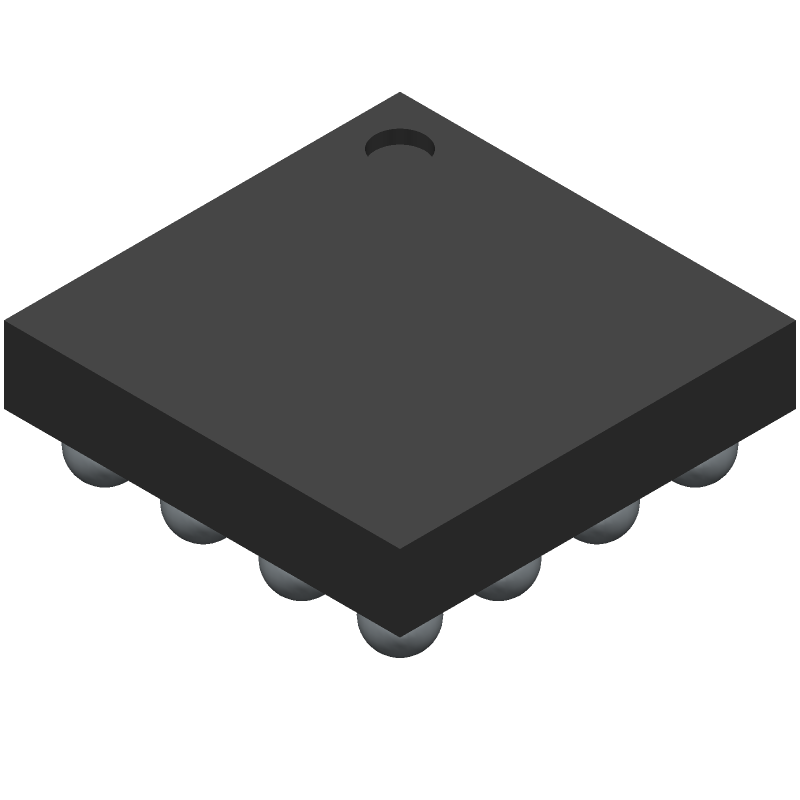
3D Model
Available Download Formats
By downloading CAD models, you agree to our Terms & Conditions and Privacy Policy

IC FPGA 10 I/O 16WLCSP
Tip: Data for a part may vary between manufacturers. You can filter for manufacturers on the top of the page next to the part image and part number.
ICE40UL1K-SWG16ITR1K by Lattice Semiconductor Corporation is a Field Programmable Gate Array.
Field Programmable Gate Arrays are under the broader part category of Programmable Logic Devices.
Programmable Logic Devices (PLDs) are reconfigurable digital components that can be customized for different applications, offering flexibility and improved performance over fixed logic devices. Read more about Programmable Logic Devices on our Programmable Logic part category page.
| Part # | Distributor | Description | Stock | Price | Buy | |
|---|---|---|---|---|---|---|
|
DISTI #
54AJ9753
|
Newark | Ice40 Ultralite , Low Cost Solution Form Of Ice40 Family, 1.2V Rohs Compliant: Yes |Lattice Semiconductor ICE40UL1K-SWG16ITR1K RoHS: Compliant Min Qty: 1000 Package Multiple: 1 Date Code: 0 Container: Reel | 0 |
|
$2.5900 / $3.3000 | Buy Now |
|
DISTI #
220-2228-1-ND
|
DigiKey | IC FPGA 10 I/O 16WLCSP Min Qty: 1 Lead time: 16 Weeks Container: Digi-Reel®, Cut Tape (CT), Tape & Reel (TR) |
694 In Stock |
|
$2.6250 / $3.3000 | Buy Now |
|
DISTI #
842-40UL1KSWG16ITR1K
|
Mouser Electronics | FPGA - Field Programmable Gate Array FPGA iCE40-UltraLite 1.2V WLCS PKG RoHS: Compliant | 1191 |
|
$2.6200 / $3.3000 | Buy Now |
|
|
Flip Electronics | Stock | 1000 |
|
RFQ |
By downloading CAD models, you agree to our Terms & Conditions and Privacy Policy
|
|
ICE40UL1K-SWG16ITR1K
Lattice Semiconductor Corporation
Buy Now
Datasheet
|
Compare Parts:
ICE40UL1K-SWG16ITR1K
Lattice Semiconductor Corporation
IC FPGA 10 I/O 16WLCSP
|
| Pbfree Code | Yes | |
| Rohs Code | Yes | |
| Part Life Cycle Code | Active | |
| Ihs Manufacturer | LATTICE SEMICONDUCTOR CORP | |
| Package Description | WLCSP-16 | |
| Reach Compliance Code | compliant | |
| Samacsys Manufacturer | Lattice Semiconductor | |
| Clock Frequency-Max | 105.2 MHz | |
| Combinatorial Delay of a CLB-Max | 9 ns | |
| JESD-30 Code | S-PBGA-B16 | |
| Length | 1.409 mm | |
| Number of CLBs | 156 | |
| Number of Inputs | 10 | |
| Number of Logic Cells | 1248 | |
| Number of Outputs | 10 | |
| Number of Terminals | 16 | |
| Operating Temperature-Max | 100 °C | |
| Operating Temperature-Min | -40 °C | |
| Organization | 156 CLBS | |
| Package Body Material | PLASTIC/EPOXY | |
| Package Code | VFBGA | |
| Package Equivalence Code | BGA16,4X4,14 | |
| Package Shape | SQUARE | |
| Package Style | GRID ARRAY, VERY THIN PROFILE, FINE PITCH | |
| Packing Method | TR | |
| Peak Reflow Temperature (Cel) | NOT SPECIFIED | |
| Programmable Logic Type | FIELD PROGRAMMABLE GATE ARRAY | |
| Seated Height-Max | 0.491 mm | |
| Supply Voltage-Max | 1.26 V | |
| Supply Voltage-Min | 1.14 V | |
| Supply Voltage-Nom | 1.2 V | |
| Surface Mount | YES | |
| Technology | CMOS | |
| Terminal Form | BALL | |
| Terminal Pitch | 0.35 mm | |
| Terminal Position | BOTTOM | |
| Time@Peak Reflow Temperature-Max (s) | NOT SPECIFIED | |
| Width | 1.409 mm |
Lattice provides a PCB design guide and layout recommendations in their documentation, including the 'PCB Design Guide for Lattice FPGAs' and 'ICE40 UltraLite FPGA PCB Design and Layout Guidelines'. Additionally, it's recommended to follow general high-speed PCB design best practices, such as using a solid ground plane, minimizing signal trace length, and using differential pairs for high-speed signals.
The ICE40UL1K-SWG16ITR1K requires a 1.2V core voltage and 3.3V I/O voltage. A recommended power supply design includes using a low-dropout regulator (LDO) for the core voltage and a separate voltage regulator for the I/O voltage. Additionally, decoupling capacitors should be placed close to the FPGA to reduce noise and ensure stable operation.
The ICE40UL1K-SWG16ITR1K has two built-in PLLs that can be used to generate clock signals. However, there are limitations on the PLL's input frequency range, output frequency range, and jitter performance. Additionally, the PLLs may not be suitable for high-frequency clock generation or applications requiring very low jitter. It's recommended to consult the datasheet and application notes for specific guidelines and considerations.
To optimize power consumption, it's recommended to use the FPGA's built-in power management features, such as dynamic voltage and frequency scaling, and to minimize the use of unnecessary resources. Additionally, using a lower clock frequency, reducing the number of active resources, and using power-saving modes can help reduce power consumption and heat generation.
To implement a reliable and secure boot mechanism, it's recommended to use a secure boot loader, such as Lattice's Secure Boot, and to follow best practices for secure firmware development, such as using encryption and secure authentication mechanisms. Additionally, it's recommended to use a non-volatile memory device, such as a flash memory, to store the FPGA's configuration data.