-
Part Symbol
-
Footprint
-
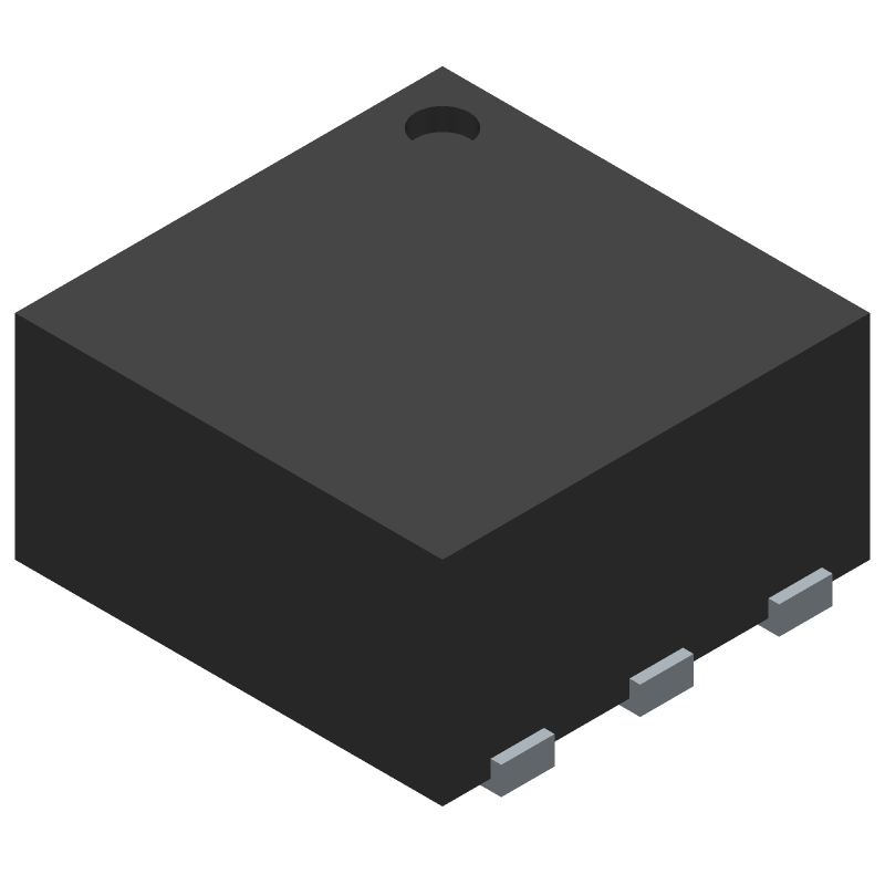
3D Model
Available Download Formats
By downloading CAD models, you agree to our Terms & Conditions and Privacy Policy
HMC536LP2
Tip: Data for a part may vary between manufacturers. You can filter for manufacturers on the top of the page next to the part image and part number.
HMC536LP2 by Analog Devices Inc is an RF/Microwave Switch.
RF/Microwave Switches are under the broader part category of RF and Microwave Components.
RF and Microwave Engineering focuses on the design and operation of devices that transmit or receive radio waves. The main distinction between RF and microwave engineering is their wavelength, which influences how energy is transmitted and used in various applications. Read more about RF and Microwave Components on our RF and Microwave part category page.
| Part # | Distributor | Description | Stock | Price | Buy | |
|---|---|---|---|---|---|---|
|
DISTI #
19AM5214
|
Newark | Mmic Switch, 0Hz To 6Ghz, Dfn-Ep-6 Rohs Compliant: Yes |Analog Devices HMC536LP2 RoHS: Compliant Min Qty: 1 Package Multiple: 1 Date Code: 1 Container: Bulk | 103 |
|
$10.0400 / $14.8700 | Buy Now |
|
DISTI #
584-HMC536LP2
|
Mouser Electronics | RF Switch ICs 3W SPDT T/R Switch SMT, DC - 6 GHz RoHS: Not Compliant | 114 |
|
$6.4400 / $12.6300 | Buy Now |
|
|
Analog Devices Inc | 3W SPDT T/R Switch SMT, DC - 6 Package Multiple: 1 | 11 |
|
$4.7300 / $12.1000 | Buy Now |
|
DISTI #
87254002
|
Verical | RF Switch SPDT 0MHz to 6GHz 23dB 6-Pin DFN EP T/R RoHS: Not Compliant Min Qty: 12 Package Multiple: 12 Date Code: 2447 | Americas - 12 |
|
$12.7797 | Buy Now |
|
DISTI #
HMC536LP2
|
Richardson RFPD | RF AND MICROWAVE SWITCH RoHS: Not Compliant Min Qty: 105 | 0 |
|
$6.1800 / $6.4400 | Buy Now |
By downloading CAD models, you agree to our Terms & Conditions and Privacy Policy
|
|
HMC536LP2
Analog Devices Inc
Buy Now
Datasheet
|
Compare Parts:
HMC536LP2
Analog Devices Inc
HMC536LP2
|
| Pbfree Code | No | |
| Rohs Code | No | |
| Part Life Cycle Code | Active | |
| Ihs Manufacturer | ANALOG DEVICES INC | |
| Package Description | 2 X 2 MM, LEADLESS, PLASTIC, SMT, DFN-8 | |
| Pin Count | 6 | |
| Manufacturer Package Code | HCP-6-1 | |
| Reach Compliance Code | not_compliant | |
| ECCN Code | EAR99 | |
| HTS Code | 8542.39.00.01 | |
| Samacsys Manufacturer | Analog Devices | |
| Characteristic Impedance | 50 Ω | |
| Construction | COMPONENT | |
| Input Power-Max (CW) | 29 dBm | |
| Insertion Loss-Max | 1.3 dB | |
| Isolation-Min | 23 dB | |
| JESD-609 Code | e0 | |
| Mounting Feature | SURFACE MOUNT | |
| Number of Functions | 1 | |
| Number of Terminals | 6 | |
| On Time-Nom | 0.07 µs | |
| Operating Frequency-Max | 6000 MHz | |
| Operating Frequency-Min | ||
| Operating Temperature-Max | 85 °C | |
| Operating Temperature-Min | -40 °C | |
| Package Body Material | PLASTIC/EPOXY | |
| Package Equivalence Code | SOLCC6,.08,25 | |
| Power Supplies | 5 V | |
| RF/Microwave Device Type | SPDT | |
| Surface Mount | YES | |
| Technology | GAAS | |
| Terminal Finish | Tin/Lead (Sn/Pb) | |
| VSWR-Max | 1.22 |
The HMC536LP2 requires careful PCB layout and thermal management to achieve optimal performance. A recommended layout is to use a 4-layer PCB with a solid ground plane, and to place the device near the edge of the board to minimize thermal resistance. Additionally, a heat sink or thermal pad can be used to dissipate heat. Refer to the application note AN-1369 for more details.
The biasing and tuning of the HMC536LP2 depend on the specific application and frequency range of operation. Analog Devices provides a simulation tool, ADIsimPLL, which can be used to optimize the biasing and tuning of the device. Additionally, the device evaluation board and software development kit (SDK) can be used to experiment with different biasing and tuning configurations.
The HMC536LP2 has excellent phase noise and spurious performance, but there are limitations to consider. The device has a typical phase noise of -230 dBc/Hz at 10 kHz offset, and a typical spurious performance of -70 dBc. However, these specifications can be affected by factors such as PCB layout, power supply noise, and temperature. Refer to the datasheet and application notes for more details.
The HMC536LP2 is a rugged and reliable device, but it still requires proper handling and storage to ensure its reliability in harsh environments. The device should be stored in a dry, cool place, and handled with care to avoid mechanical stress and electrostatic discharge (ESD). Additionally, the device should be operated within its recommended operating conditions, and proper thermal management should be implemented to prevent overheating.
The HMC536LP2 is a complex device, and there are several potential sources of error, including phase noise, spurious signals, and temperature drift. These errors can be mitigated by using proper PCB layout and thermal management, optimizing the biasing and tuning of the device, and using external filters and amplifiers to improve the signal-to-noise ratio. Additionally, the device evaluation board and SDK can be used to experiment with different configurations and optimize the performance of the device.